

Atomic-level sensors enable measurements of electric field
The proper functioning of semiconductor devices relies on their internally generated electric fields. Being able to measure these fields on the nanoscale is crucial for the development of next gen electronics, but present techniques have been restricted to measurements of the electric field at a semiconductor’s surface. A group of Takayuki Iwasaki, Mutsuko Hatano and colleagues at the Tokyo Institute of Technology, the Japan Science and Technology Agency (JST) and Toshiharu Makino at the National Institute of Advanced Industrial Science and Technology (AIST) has reported a new method for sensing internal electric fields at the interior of operating semiconductor devices. The technique exploits the response of an artificially introduced single electron spin to variations in its surrounding electric field, and enabled the researchers to study a semiconductor diode subject to bias voltages of up to 150V.
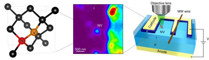
Iwasaki and co-workers applied their method to diamond, a so-called wide-band-gap semiconductor in which the electric fields can become very strong — a property important for low-loss electronic applications. Diamond has the advantage that it easily accommodates nitrogen-vacancy (NV) centers, a type of point defect that arises when two neighboring carbon atoms are removed from the diamond lattice and one of them is replaced by a nitrogen atom. NV centers can be routinely created in diamond by means of ion implantation. A nearby electric field affects an NV center’s energy state, which in turn can be probed by a method called optically detected magnetic resonance (ODMR).
The researchers first fabricated a diamond p-i-n diode (an intrinsic diamond layer sandwiched between an electron- and a hole-doped layer) embedded with NV centers. They then localized an NV center in the bulk of the i-layer, several hundreds of nanometers away from the interface, and recorded its ODMR spectrum for increasing bias voltages. From these spectra, values for the electric field could be obtained using theoretical formulas. The experimental values were then compared with numerical results obtained with a device simulator and found to be in good agreement – confirming the potential of NV centers as local electric-field sensors.
Iwasaki and colleagues explain that the experimentally determined value for the electric field around a given NV center is essentially the field’s component perpendicular to the direction of the NV center – aligned along one of four possible directions in the diamond lattice. They reason that a regular matrix of implanted NV centers should enable reconstructing the electric field with a spatial resolution of about 10nm by combining with super-resolution techniques, which is promising for studying more complex devices in further studies.
The researchers also point out that electric-field sensing is not only relevant for electronic devices, but also for electrochemical applications: the efficiency of electrochemical reactions taking place between a semiconductor and a solution depends on the former’s internal electric field. In addition, Iwasaki and co-workers note that their approach need not be restricted to NV centers in diamond: similar single-electron-spin structures exist in other semiconductors like e.g. silicon carbide.
Background
Wide-band-gap semiconductors
Semiconducting materials feature a so-called band gap: an energy range wherein no accessible energy levels exist. In order for a semiconductor to conduct, electrons must acquire sufficient energy to overcome the band gap; controlling electronic transitions across the band gap forms the basis of semiconducting device action. Typical semiconductors like silicon or gallium arsenide have a band gap of the order of 1 electron volt (eV). Wide-band-gap semiconductors, like diamond or silicon carbide, have a larger band gap — values as high as 3-5eV are not uncommon.
Due to their large band gap, wide-band-gap semiconductors can operate at temperatures over 300°C. In addition, they can sustain high voltages and currents. Because of these properties, wide-band-gap semiconductors have many applications, including light-emitting diodes, transducers, alternative-energy devices and high-power components. For further development of these and other future applications, it is essential to be able to characterize wide-band-gap devices in operation. The technique proposed by Iwasaki and colleagues for measuring the electric field generated in a wide-band-gap semiconductor subject to large bias voltages is therefore a crucial step forward.
Nitrogen-vacancy centers
Diamond consists of carbon atoms arranged on a lattice where each atom has four neighbors forming a tetrahedron. The diamond lattice is prone to defects; one such defect is the nitrogen-vacancy (NV) center, which can be thought of as resulting from replacing a carbon atom with a nitrogen atom and removing one neighboring carbon atom. The energy level of an NV center lies in the band gap of diamond but is sensitive to its local environment. In particular, the so-called nuclear hyperfine structure of an NV center depends on its surrounding electric field. This dependence is well understood theoretically, and was exploited by Iwasaki and co-workers: detecting changes in an NV center’s hyperfine structure enabled them to obtain values for the local electric field. A major advantage of this approach is that it allows monitoring the field within the material – not just at the surface, for which methods had already been developed.
Optically-detected magnetic resonance
For probing the nuclear hyperfine structure of an NV center in the bulk of the diamond-based device, Iwasaki and colleagues employed optically detected magnetic resonance (ODMR): by irradiating the sample with laser light, the NV center was optically excited, after which the magnetic resonance spectrum could be recorded. An electric field makes the ODMR resonance split; the experimentally detected split width provides a measure for the electric field.
More information: EurekAlert!