
New semiconducting material may lead to faster electronics
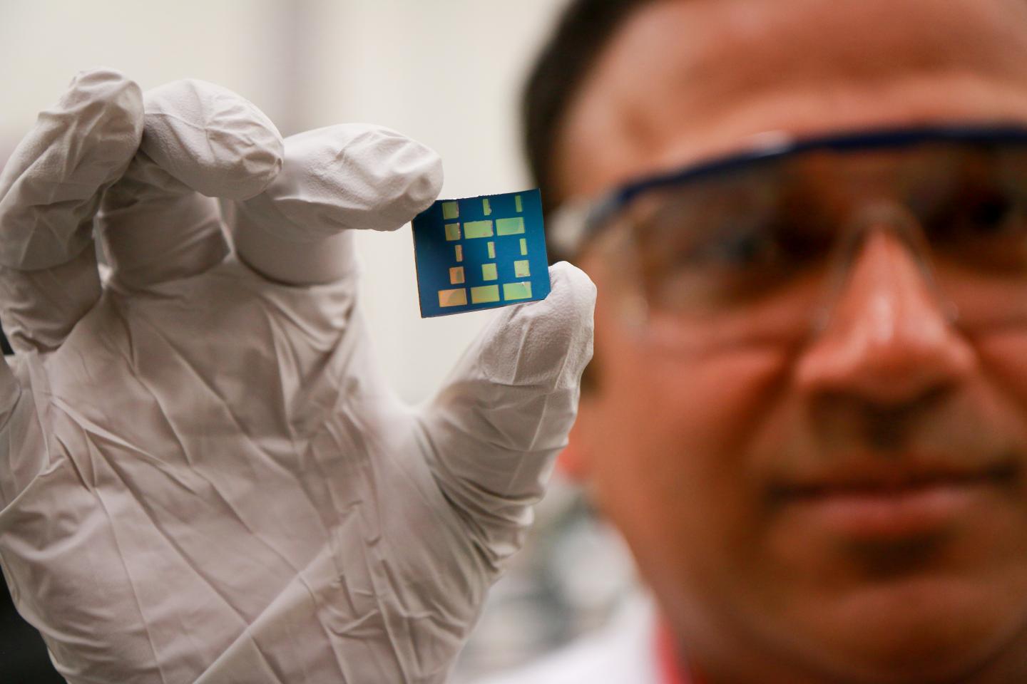
A typical computer processor is comprised of billions of transistors, and the more transistors that can be packed into a single chip, the more powerful the processor can become. Well, engineers from the University of Utah have discovered a new semiconducting material that could be used in transistors to create faster electronics devices, like computers and smartphones, that consume less power.
The semiconductor, a 2D layers only one atom thick, was made of tin and oxygen, also known as tin monoxide (SnO) and allows electrical charges to move through it much faster than conventional 3D materials such as silicon.
Currently, transistors and other components used in electronic devices are made of 3D materials like silicon and consist of multiple layers on a glass substrate. However, 3D materials allow for electrons to bounce around in all different directions, while 2D materials (discovered just about five years ago) only permit electrons to move within one layer — and prove to be much faster.
There are other kinds of 2D material being worked on by researchers, such as graphene, molybdenun disulfide and borophene, but they only allow the movement of negative electrons. In order to create an electronic device, you would need semiconductor material that allows the movement of both negative electrons and positive charges known as “holes.” The tin monoxide material discovered by the University of Utah team is the first stable P-type 2D semiconductor material ever in existence.
“Now we have everything, we have P-type 2D semiconductors and N-type 2D semiconductors,” said Ashutosh Tiwar, associate professor of engineering who led the research. “Now things will move forward much more quickly.”
Tiwari’s new 2D material can lead to the manufacturing of transistors that are even smaller and faster than those in use today, creating computers and smartphones that are 100 times faster than ordinary devices. Another added bonus of the new material: the electrons will move through only one layer creating less friction and therefore not getting as hot as normal computer chips. They also will require much less power to run.
According to Tiwari, this could be important for medical devices such as electronic implants that will run longer on a single battery charge.
“The field is very hot right now, and people are very interested in it,” said Tiwari. “So in two or three years we should see at least some prototype device.”
Comments are closed, but trackbacks and pingbacks are open.