
The first colorless and bendable semiconducting material
A “sweet spot” for organic electronics may have been found by researchers by fabricating a new 2D semiconducting polymer-blended nanonetwork material that simultaneously achieves excellent charge mobility, high flexibility, and nearly 100% optical transparency—a combination of properties that has so far been elusive for semiconducting materials. According to the researchers, the nanonetwork is the first truly colorless, bendable semiconducting material, as demonstrated by the fabrication of field-effect transistors with integrated LEDs.
The researchers, led by Kwanghee Lee, a professor at the Gwangju Institute of Science and Technology in South Korea, have published a paper on the new material in the Proceedings of the National Academy of Sciences.
“So far, there has been no semiconducting material that simultaneously achieves excellent optical transparency, high charge-carrier mobility, and real flexibility,” coauthor Kilho Yu at the Gwangju Institute of Science and Technology told Phys.org. “Metal oxides, such as ZnO and IGZO, have excellent transparency and high mobility, but they are brittle and show poor mobility if not treated with high-temperature (>200°C) processes, which are not desirable for fabrication on flexible substrates. General semiconducting polymers are flexible, but show poor mobility without complex processes and are not very transparent because of their high optical absorption coefficient.”
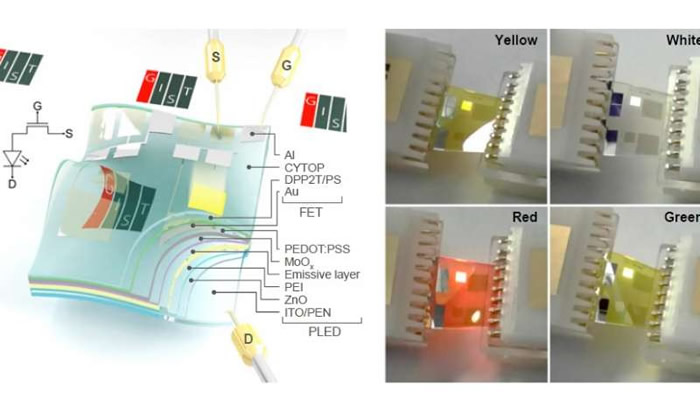
The new polymer blend consists of about 15% semiconducting polymer called DPP2T integrated into an inert polystyrene matrix. The two types of polymers do not mix uniformly, but instead the DPP2T forms a web-like nanonetwork through the inert matrix, creating highly ordered, continuously connected charge pathways for rapid charge transport.
So far, transparency has been particularly challenging to achieve in semiconducting polymers because of their inherently high light absorption in the visible range. DPP2T belongs to a newer class of semiconducting polymers in which the light absorption peak is red-shifted to the near-infrared range, so it absorbs much less light in the visible range and has greater optical transparency.
However, DPP2T by itself still has a greenish tint. Only by blending the DPP2T with the polystyrene matrix could the researchers fabricate a material that is almost perfectly transparent throughout the visible range.
In the final analysis, the researchers showed that the individual materials in the polymer blend cannot achieve all three of the desired properties on their own, but only when blended together.
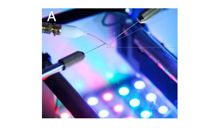
To demonstrate, the researchers fabricated prototypes of colorless, bendable field-effect transistors integrated on top of colorless, bendable light-emitting diodes. The devices could withstand 1,000 bending cycles with no severe performance degradation.
“The nanonetwork semiconductor can be made very easily and is solution-processable, and it needs no heat treatment or any other complex processes,” Yu said. “It simultaneously achieves excellent characteristics for future transparent, deformable electronic applications. The applicability of the nanonetwork semiconductor was proven by the fabrication drive of prototype FET/OLED integrated devices. In the paper, we also have shown a new paradigm for achieving facile charge transport in semiconducting polymers, which emphasizes the importance of clean charge pathways along the polymer backbone, rather than the degree of crystallinity of the polymer.”
The researchers expect that the results will pave the way for the development of a wide variety of applications, such as next-generation “see-through” bendable electronics and skin-attachable medical devices.
“We are currently investigating the intriguing charge transport mechanism of the nanonetwork semiconductor using various experimental tools and modeling,” Yu said. “In addition, we are applying this nanonetwork semiconductor toward various electronic applications, in order to make it a platform technology for deformable and transparent electronics.”
More information: Phys.org
Comments are closed, but trackbacks and pingbacks are open.