
First Programmable ASSP (pASSP) Interface Bridge
Lattice Semiconductor announced the industry’s first Lattice CrossLinkTM programmable bridging device that supports leading protocols for mobile image sensors and displays. Systems with embedded cameras and displays often do not have the right type or number of interfaces, which can be resolved using a bridge. The new CrossLink device combines the flexibility and fast time to market of an FPGA with the power and functional optimization of an ASSP to create a new product class called programmable ASSP (pASSPTM). As the first product in this category, the CrossLink device is a low cost video interface bridge with the highest bandwidth, lowest power and smallest footprint. This makes it the optimal solution for virtual reality headsets, drones, smartphones, tablets, cameras, wearable devices and human machine interfaces (HMIs).
The CrossLink device’s features include:
– World’s fastest MIPI D-PHY bridging device that delivers up to 4K UHD resolution at 12 Gbps bandwidth.
– Supports popular mobile, camera, display and legacy interfaces such as MIPI D-PHY, MIPI CSI-2, MIPI DSI, MIPI DPI, CMOS, and SubLVDS, LVDS and more.
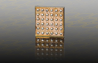
– Industry’s smallest package size with a 6 mm2 option.
– Lowest power programmable bridging solution in active mode.
– Built-in sleep mode.
– Takes the strongest features from ASSPs and FPGAs to deliver the best solution of both worlds.
“The latest wave of image capture and display technology, including drones and VR, is creating real industry excitement. Combining these new technologies with a global base of 3.7 billion smartphones and tablets that’s set to rise more than 30 percent by 2020, all equates to a wide variety of interfaces that must be integrated to ensure compatibility,” said Carl Hibbert, associate director of entertainment content and delivery, Futuresource Consulting. “The ability to manage these interfaces through a low cost, low power and small footprint bridging solution is essential.”
Bridging the Video Connectivity Gap
Image Sensor Applications
Lattice’s CrossLink bridge can multiplex, merge and arbitrate between multiple image sensors to a single input. The device can also interface between high-end industrial and popular A/V image sensors with mobile application processors. This is ideal for 360, action, surveillance and DSLR cameras along with drones, augmented reality products and more.
Display Applications
With the CrossLink device, it is possible to receive video data from one MIPI DSI interface and send it out over two MIPI DSI interfaces at half the bandwidth. The same video stream can be split to two interfaces, ideal for virtual reality headsets and mobile set top boxes. Customers can also integrate consumer and industrial panels with RGB or LVDS interfaces with mobile applications processors. The CrossLink bridge can convert from MIPI DSI to multiple lanes of CMOS or LVDS interfaces such as MIPI DPI, OpenLDI and proprietary interface formats for HMIs, smart displays, smart homes and more.
“The CrossLink bridge has the flexibility of an FPGA and the performance of an ASSP for video technologies,” said C.H. Chee, senior director of consumer product marketing, Lattice Semiconductor. “Our product has a variety of applications for high-volume growth segments that demand fast, flexible innovation and solves the pressing challenge of having too many incompatible interfaces on one device.”
Comments are closed, but trackbacks and pingbacks are open.