Marktech Optoelectronics announces expanded manufacturing capabilities
Marktech Optoelectronics has announced the expanded photodetector design and manufacturing capabilities of Marktech West, its fully dedicated second facility in Simi Valley, California, USA.
Established in 2015, the 3,800ft2 Marktech West offers all the necessary infrastructure, technology, and engineering expertise for the design, development and manufacture of high-reliability photodetectors, in quantities ranging from prototype to OEM volumes, from wafer design stage up thru complete subsystems. Extensive Marktech investments in advanced production technology and equipment, including a Class 1,000 (ISO 6) cleanroom, have created a highly controlled manufacturing environment in which to produce both Silicon (Si) and Indium Gallium Arsenide (InGaAs) photodetectors of the highest possible quality. Available offerings, each with extensive front- and back-end customization capabilities, include:
- UV detectors, with spectral sensitivities from 150 to 570nm, and further incorporating Gallium Phosphide (GaP), Gallium Nitride (GaN) and Silicon Carbide (SiC) materials, for superior long-term stability, high device sensitivity and low dark current;
- Silicon photodiodes and silicon phototransistors, with spectral sensitivities from 350 to 1,100nm, for visible and NIR applications requiring low noise, high speed and high sensitivity. Silicon wafers and chips are optimized to ensure uniform, consistent performance and high reliability. Available cost-effective customization capabilities to exacting standards include wavelength specific band-pass filtering, and hybridization.
- Avalanche Photodiodes (APD’s), featuring higher sensitivities than standard photodiodes, for high-accuracy, Low-Level Light (LLL) detection, short pulse detection, and applications requiring higher bandwidth or internal gain, as required to overcome high preamplifier noise levels. Standard Marktech APD’s offer an internal gain mechanism, fast rise times, low dark current, and high NIR spectral sensitivity. Available cost-effective customization options to exacting standards include operational voltage selection (Vbr binning), wavelength specific band-pass filtering, and hybridization. Silicon-based APD’s (Si APD’s), supporting high-speed and low-light-level NIR optical detection from 400 to 1,100nm, are offered with active area sizes of 230 and 500um, and with peak response optimization of either 800 or 905nm.
- 100% US-based custom silicon chip and wafer design and processing, with designs for long-term stability, radiation hardness and high-reliability against UV and Gamma radiation.
- GaP Schottky photodetectors, specially optimized for high-accuracy UV photodetection up to the visible spectrum, 150 to 550nm.
- Standard photovoltaic or photoconductive silicon photodiodes, with spectral sensitivities from 350 to 1,100nm, for applications requiring high-broadband sensitivity, moderate-to-fast response speeds, and optimized spectral enhancements.
- InGaAs PIN photodiode chips, in active area sizes from 0.1 to 3.0mm, with spectral sensitivities from 800 to 2,600nm. Marktech InGaAs PIN photodiode chips offer an optimal balance between low dark current, high speed and light sensitivity. No thermoelectric cooling is utilized in the manufacturing of Marktech PIN photodiodes, thereby reducing costs and improving overall efficiencies.
- Foundry services, for the epitaxial growth of high-reliability SWIR wafers in the 1.0 to 2.6μm range, with InP material as the base substrate, in 2, 3 and 4″ diameters.
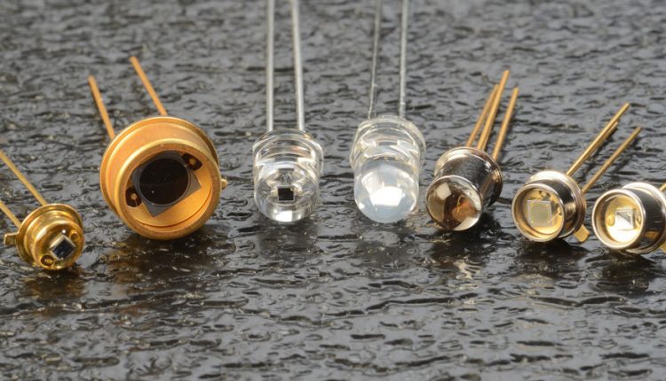
Additional facility capabilities include mask design, custom packaging, and hybrid electronic designs. Front-end customization options include chip geometry design flexibility; responsivity to operating wavelengths; rise times to unique bandwidths; capacitance, for reduced noise and increased speed; dark current, for improved dynamic range; and anti-reflective coatings, for reduced optical losses. Back-end customization capabilities to unique environmental requirements include filter-in packages, for reduced ambient light effects; optical component add-ons, such as optical lenses, scintillators, etc.; light sources, including LEDs or laser dice for assembly miniaturization; integration of heaters, coolers, temperature sensors and op-amps; and custom packaging. Photodetectors are typically packaged within a variety of transistor metal case styles, in sizes from TO-18 to B-1032. Optoelectronic modules are further offered for simplified application integration and evaluation.
Marktech Optoelectronics president, Bill Moore noted: “We are pleased to announce our expanded West Coast photodetector manufacturing capabilities, established for the added convenience of our valued customers. These capabilities now allow us to manufacture a variety of photodetectors with highly competitive lead times, in anywhere from prototype to OEM volumes, using the very latest equipment and manufacturing processes. We look forward to continuing to advance our in-house manufacturing capabilities, in response to customer needs.”

