


In most design discussions, the focus tends to stay on the silicon. People talk about switching speeds, device structure, thermal limits and how far a node can be pushed. But once that IC ends up on a board, a lot of what you actually experience in the system has nothing to do with the transistor geometry at all. It often comes down to something much simpler: how the part is packaged.
Texas Instruments recently published a white paper that walks through this idea in detail and looks at several packaging approaches the company uses in its analog and power portfolio. The paper explains how the package affects thermal behavior, switching performance, reliability and even board layout choices. After going through the material, it’s clear that packaging has become a bigger part of overall system performance than many engineers realize.
Most conversations about improving analog performance still revolve around what happens inside the silicon. Faster devices, better architectures and smaller geometry all matter. TI’s paper points out that the package around the die often shapes the final behavior of the part just as much, especially in high current or compact systems.
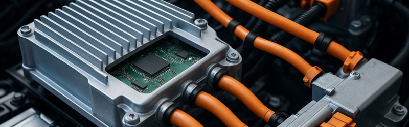
Traditional wirebond packages are still widely used, but they come with some limitations. The bond wires add resistance and inductance that can show up as heat, noise or slower switching edges. This might not be a problem in low current applications, but it becomes more noticeable in power conversion and motor-drive designs. TI explains how using copper clips or copper bumps instead of long wirebonds creates a lower resistance, lower inductance path. This helps reduce losses and improves thermal performance in a way the silicon alone cannot achieve.
The paper also describes TI’s HotRod packaging. In this style, the die connects more directly to copper inside the package, which lowers inductance and leads to cleaner switching. Engineers working on fast power stages often deal with ringing and EMI caused by parasitics they didn’t anticipate. Reducing those parasitics at the package level can simplify layout and make the system easier to stabilize. It also lets the IC perform closer to its intended capabilities.
Size is another major theme. The paper highlights chip-scale packaging and other formats intended for wearable devices, compact sensors and other designs where space is extremely limited. These small packages aren’t only about saving board space. The short internal paths can reduce mechanical stress on the die and improve signal consistency. That gives the designer a part that is both smaller and more predictable.
Another interesting section of the paper looks at integrating passive components inside the package. TI uses MagPack as an example, where inductors are built into the same package as the IC. This reduces board area and also reduces the amount of variation that comes from selecting and placing external magnetics. The smaller magnetic loop inside the package can improve EMI behavior and produce a cleaner power stage.
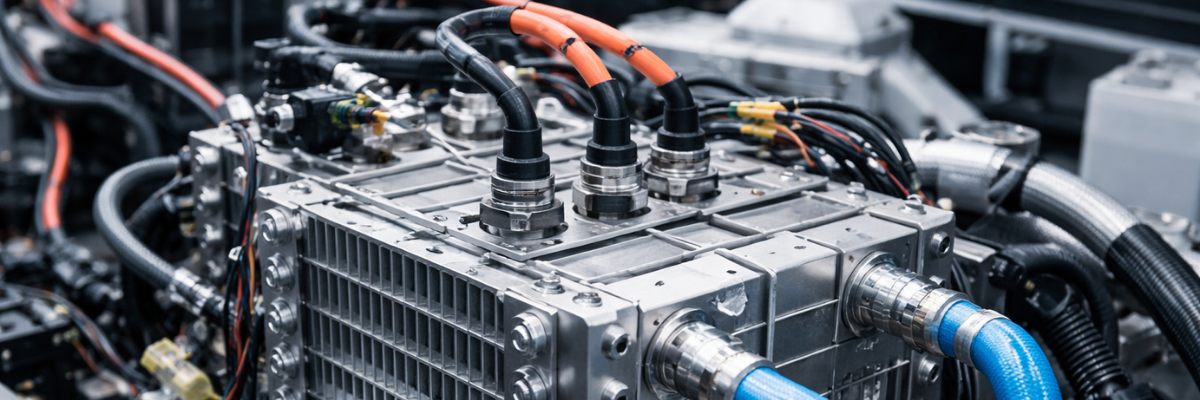
Reliability becomes a big topic too, especially for automotive, industrial and high-voltage systems. A package may work fine in a clean lab, but real-world conditions can be harsh. Vibration, humidity, long-term thermal cycling and electrical stress all take a toll. TI outlines how different mold compounds, spacing techniques and ceramic options are used for parts that need to survive long operating lifetimes or challenging environments. These details can determine whether a device continues to meet spec over years of operation.
The overall message from the paper is that packaging affects system performance in many small but important ways. If the package introduces too much inductance or resistance, the engineer ends up solving problems later through layout changes, thermal solutions or derating. If the package is well matched to the application, the design becomes easier and more efficient.
Some practical points designers can take from the paper include:
• For high current or fast switching applications, packages with copper clips or low-inductance structures can reduce losses and noise.
• For space-limited designs, chip-scale packages offer both small size and good electrical behavior.
• For automotive and industrial use, it is important to check long-term reliability data and understand how the package handles stress.
• For precision analog circuitry, internal mechanical stress inside the package can affect drift and offset, so package type matters.
TI’s white paper makes the case that packaging is not just the outer container of an IC. It is a part of the design that shapes electrical, thermal and mechanical performance. As systems keep pushing for higher density and tougher operating conditions, packaging is becoming one of the key tools that enable better results without relying solely on changes to the silicon itself.
Texas Instruments. “Accelerating Analog Performance With Packaging Breakthroughs.”