


Longsys has unveiled what it calls the industry’s first micro SSD (mSSD) built with an integrated-packaging design. The new product merges the controller, NAND flash and power management IC (PMIC) into a single system-in-package (SiP) module. By doing so, the company eliminates nearly 1,000 solder joints that are found in conventional printed-circuit-board-assembly (PCBA) SSDs.
From a manufacturing standpoint, this is significant. Fewer solder joints means lower risk of failures due to solder contamination, component interference or thermal/humidity stress. Longsys reports the defects per million (DPPM) rate drops from 1,000 or more to 100 or fewer with this design.
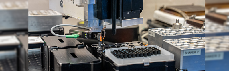
The manufacturing flow changes as well. Traditional SSD packaging involves printed circuit boards, component placement, reflow soldering, and multiple transfer and mounting steps. Longsys shifts to a one-step packaging process: the SiP module is assembled as a single unit prior to final integration. This approach doubles delivery efficiency and reduces cost by more than 10 percent, while also cutting energy use and carbon emissions in manufacturing.
On the product side, the mSSD comes in an ultra-compact form factor: 20 × 30 × 2.0 mm and around 2.2 g. Despite the small size, the device supports PCIe Gen4 ×4 performance, achieving sequential read speeds up to 7,400 MB/s and sequential write speeds up to 6,500 MB/s. Thermal design uses materials such as high-conductivity aluminum alloy, graphene and conductive silicone to maintain stable full-speed operation — making it suitable for high-end applications like AI PCs, gaming handhelds, drones and VR devices. The device meets NVMe L1.2 low-power mode with standby power consumption at or below 3.5 mW.
Capacity options span from 512 GB up to 4 TB and the module supports TLC or QLC NAND. For form-factor flexibility, Longsys includes a clip-on thermal expansion card that enables conversion between M.2 2230, 2242 and 2280 standards. The company also enables on-site customization through ink-jet or UV printing of device surfaces, highlighting its “Office is Factory” manufacturing model.
For product engineers and OEMs, the key takeaways are: a dramatically reduced component count, board space saved, simplified assembly, and high performance in a low-profile package. The SiP approach means fewer soldering steps, less risk in manufacturing, and higher consistency in product quality.
The initiative aligns with industry trends toward compact, high-performance storage in embedded systems, edge compute and consumer devices that demand high throughput, low power and minimal size. While the SiP architecture brings advantages, engineering teams will still need to validate integration with their system thermal and mechanical environments, evaluate endurance and serviceability, and assess cost at scale relative to more traditional SSD modules.