


At the 2016 IEEE International Electron Devices Meeting, in a special poster session on MRAM, imec presented an 8nm p-MTJ device with 100% tunnel magnetoresistance (TMR) and coercive field as high 1500Oe. This world’s smallest device enables the establishment of a manufacturing process for high-density spin-transfer-torque magnetic random access memory (STT-MRAM) arrays that meet the requirements of the 10nm and beyond logic node for embedded non-volatile memory applications. It also paves the way for high density stand-alone applications.
STT-MRAM has the potential to become the first embedded non-volatile memory technology on advanced logic nodes for advanced applications and is also considered an alternative to conventional dynamic random access memory (DRAM). The core element of an STT-MRAM is a magnetic tunnel junction (MTJ) in which a thin dielectric layer is sandwiched between a magnetic reference layer and a magnetic free layer, where writing of the memory cell is performed by switching the magnetization of the free layer. STT-MRAMs exhibit non-volatility, high-speed, low-voltage switching and nearly unlimited read/write endurance. However, significant challenges towards commercialization remain, primarily in scaling the processes for higher densities and in increasing the device switching current.
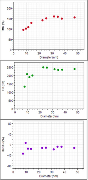
In addressing these challenges, imec scientists have demonstrated for the first time an electrical functional device as small as 8nm. Despite the small dimensions, the device exhibits a high TMR of 100 percent, a coercivity (Hc) of 1500Oe and a spin torque efficiency -the ratio of the thermal stability and switching current- as high as three. The p-MTJ stack, featuring a free layer and reference layer of CoFeB-based multilayer stacks, was developed on 300mm silicon wafers and the fabrication process is compatible with the thermal budget of standard CMOS back-end-of-line (BEOL) technology.
Moreover, imec integrated arrays of p-MTJ devices into a 1T1MTJ structure to build STT-MRAM Megabit arrays with pitches down to 100nm, proving that the technology meets the dimensional requirements for the 10nm logic node and beyond.
Imec’s research into advanced memory is performed in cooperation with imec’s key partners in its core CMOS programs including GlobalFoundries, Micron, Qualcomm, Sony and TSMC.