A new combination of methods that can provide detailed information about the microstructure of polycrystalline metals has been developed by researchers at MIT and elsewhere. Such materials—composed of a random matrix of multiple small crystals rather than one single large crystal—are widely used for such applications as nuclear reactors, civil infrastructure, and aircraft. However understanding the details of their crystal structure and the boundaries between the crystal areas has been difficult.
The findings are published in the journal Nature Computational Materials, in a paper by Matteo Seita, an MIT postdoc; Michael Demkowicz, a professor of materials science and engineering; Christopher Schuh, the Danae and Vasilis Salapatas Professor of Metallurgy, and five others.
“This is a unique combination of different technologies,” Seita explains. The approach he and the team developed addresses “one of the most common problems in materials science: How do we quantify the characteristics of materials in a high-throughput fashion?”
Some techniques offer a great deal of detail about structures, but they take time to carry out and can’t reveal rapid changes within the material.
Others work rapidly but provide much less structural detail, and still other methods provide both spatial and temporal detail but are prohibitively expensive or only available in limited places. The new combination of techniques, Seita says, can help resolve these limitations by providing fast, high-resolution, and low-cost imaging of the materials.
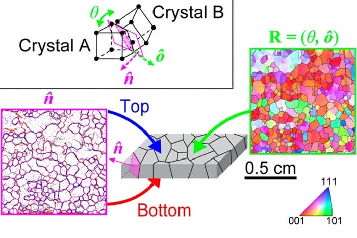
In polycrystalline metals, which are composed of many small crystal grains, it is important to know the location, dimensions, angles of contact, and other characteristics of the different grains making up the material.
In particular, the interfaces between the crystal grains, called grain boundaries, “happen to be critical,” Seita says, “to many individual properties of the material—its strength, radiation tolerance, hardness, electrical resistance, and so on—but they are very difficult to characterize experimentally, because they are very complex.”
There are five basic characteristics about these grain boundaries that researchers would like to be able to quantify, but most tools for studying the materials can only yield some subset of two or three of those.
One method for getting all five characteristics at once is high-energy synchrotron radiation, which is only available in a few facilities that are expensive and tend to be oversubscribed.
“Our solution was to try to create a very simple technology that can be used by anyone, in their own lab, using software and hardware that are easily available,” Seita says. And that’s what they achieved, using a combination of two existing methods—optical microscopy and electron microscopy.
“We take two different datasets and combine them using our numerical image analysis,” he explains. To do so, they used sheets of polycrystalline metal foil, which were thin enough that single grains could be seen from both sides.
They then took optical microscope images of the foil from one side, flipped the sheet over, and imaged the other side, and used software to connect the grain boundaries from one side to the other. From that, he says, “We can reconstruct the 3D orientation of these grain boundaries.”
Then, that information is combined with electron microscope images that describe the actual pattern of atoms within the grains, showing the orientation of the individual crystal lattices within each grain—and how they relate to those of adjacent grains. The combined information provides all five characteristics of the grain boundaries in the metal foils.
“The beauty of this is that it’s high-throughput technology,” Seita says. “On one sample, we can measure up to 500 grain boundaries or so, and can build up datasets rapidly. And it’s nondestructive,” unlike existing methods that consume the sample in the process.
That means the sample can then be subjected to other tests, for example tests of mechanical or electrical properties, whose results can be compared with the data about the grain boundaries.
The methodology, Seita says, “is very versatile, so many groups out there can use it.” What’s more, though the initial tests were done with polycrystalline metals, the technique “is materials agnostic,” and could be applied to insulators or semiconductors as well as metals. “We can test for different kinds of properties and build up large datasets,” he says, and ultimately use that data to predict the characteristics of new polycrystalline materials.
More information: Massachusetts Institute of Technology