
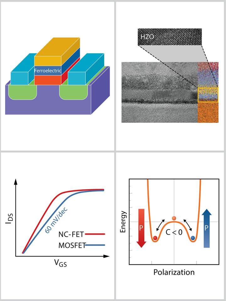
Negative capacitance field-effect transistors are being explored as a way to make traditional transistors more efficient — by simply adding a thin film of dielectric material.
Billions of tiny switches called transistors are found in your smartphone. They allow us to perform tasks like sending texts, navigating neighborhoods, snapping selfies and Googling names. These switches involve an electrically conducting channel whose conductivity can be changed by a gate terminal, which is separated from the channel by a dielectric film that’s just 5 to 6 atoms thick.
Over the past 50 years, engineers have been able to miniaturize transistors based on Moore’s law, an observation that the number of transistors on a chip can double roughly every 18 months while the cost is cut in half.
But we’ve now reached the point where transistors can’t continue to be scaled any further.
The journal Applied Physics Letters, from AIP Publishing, has released new research that reviews negative capacitance field-effect transistors (NC-FETs), a new device concept that suggests traditional transistors can be made much more efficient by simply adding a thin layer of ferroelectric material. If it works, the same chip could compute far more, yet require less frequent charging of its battery.
The physics of the technology are being assessed throughout the world and, in their article, the researchers summarize state-of-the-art work with NC FETs and the need for self-consistent and coherent interpretation of a variety of experiments being reported in the literature.
“NC FETs were originally proposed by my colleague professor Supriyo Datta and his graduate student Sayeef Salahuddin, who is now a professor at the University of California, Berkeley,” said Muhammad Ashraful Alam, a professor of electrical and computer engineering at Purdue University.
Alam found the concept of NC-FETs intriguing — not only because it addresses a pressing problem of finding a new electronic switch for the semiconductor industry, but also because it serves as a conceptual framework for a broad class of phase-transition devices collectively termed “Landau switches.”
(Image Credit: Peide D. Ye)
Alam and co-author professor Peide Ye began experimentally demonstrating these transistors, which allowed them to explore a ‘theorist-experimentalist’ perspective on the topic.
Although hundreds of papers have been published on the topic, according to the researchers, the validity of quasi-static NC and the frequency-reliability limits of NC-FET are still being hotly debated.
If conclusively demonstrated and integrated into modern ICs, the impact of the NC-FET transistors will be transformative.
“Given the potential, there is a need for systematic analysis of the device concept,” said Ye. “We found that the data from various groups has a wide scatter and researchers are using very different techniques to characterize their devices. This requires an integrated and comprehensive analysis of the existing data set.”
The researchers hope their work will bring the community together to suggest ways of making coordinated progress toward realizing this promising technology.