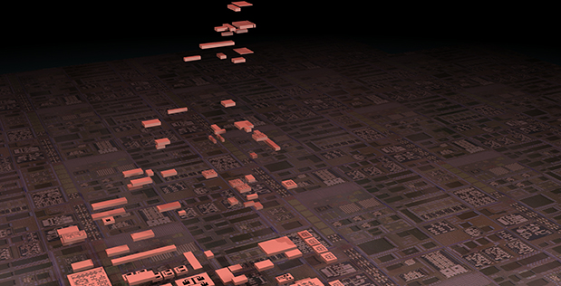
Inside of your electronic devices you’ll find a printed circuit board (PCB), a green gizmo filled with processors, memory chips, data and graphics components, among other, that are all interconnected with wire.
The Defense Advanced Research Projects Agency (DARPA) has challenged researchers and engineers to turn an ordinary PCB into a gadget the size of just one single chip in its newest program called “CHIPS“.
“We are trying to push the massive amount of integration you typically get on a printed circuit board down into an even more compact format,” said Dr. Daniel Green, manager of the new program, whose acronym, “CHIPS,” is itself a typographic feat of miniaturization; the program’s full name is the Common Heterogeneous Integration and Intellectual Property (IP) Reuse Strategies Program. “It’s not just a fun acronym,” Green said. “The program is all about devising a physical library of component chips, or chiplets, that we can assemble in a modular fashion.”
One of the main reasons DARPA aims to miniaturize the technology is to develop a new strategy for designing and building next generation microsystems, in which the time and energy it takes to move signals (data) between chips is reduced by factors of tens or even hundreds.
“This is increasingly important for the data-intensive processing that we have to do as the data sets we are dealing with get bigger and bigger,” said Green.
So far the program does not list specific applications for the miniaturized technology but the overall use could have an impact on computing efficiency and the power needed to identify objects and actions in real-time video feeds, real-time language translation, and coordinate motion on-the-fly among swarms of fast-moving unmanned aerial vehicles (UAVs).
DARPA has requested information in order to gain ideas from expert and industry players so that the CHIPS team can hone the details of the program in ways that they can be easily incorporated into existing semiconductor foundries and electronics fabrication facilities.
“Key to the success of CHIPS will be standards and interfaces, and this means we will be working with a community, not all by ourselves,” said Green.
A major part of the overall CHIPS vision is to create commercial “chiplets”—small-scale chips that individually embody a particular function, such as data storage, computation, signal processing, and managing the form and flow of data. The group envisions that integrating dozens of chiplets like a mosaic, on a so-called interposer, which is like a printed circuit board writ small, would allow the microsystems’ functions to be performed much more closely and efficiently than if they were distributed in the usual way among a suite of chips attached to a conventional PCB.