A new version of ams industry benchmark Process Design Kit (PDK) has been introduced, which features ams’ 180nm CMOS technology, that is newly to be manufactured in ams’ 200mm fabrication facility in Australia. The new PDK provides product developers with a plug-and-play tool set with improved analogue features and device performance as well as highly accurate simulation models.
 The kit facilitates first-time-right designs, which is a mission-critical capability in an industry with continuously shortening development schedules.
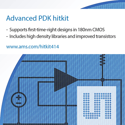
ams’ “hitkit” design environment comes with 1.8 and 5.0V NMOS and PMOS devices (substrate based, floating, low leakage and high threshold voltage options) and fully characterized passives including various capacitors. Area-optimized high-density and low-power digital libraries with gate densities up to 152kGates/mm2, updated digital and analogue I/O libraries with up to 6 metal layers as well as ESD protection cells with up to 8kV HBM level are included. One-Time Programmable (OTP) memories, online memory generation service for RAMs and ROMs as well as a Zero-Mask-Level-Adder EEPROM IP block (up to 8kb) complete the offering.
Based on Virtuoso Custom IC technology 6.1.6 from Cadence, the new hitkit helps design teams to significantly reduce time-to-market for highly competitive products in the analogue-intensive mixed-signal arena. Offering highly accurate simulation models, extraction and verification run sets for both Calibre and Assura and flexible SKILL-based PCells, the hitkit provides a comprehensive design environment and a proven route to silicon. The 180nm CMOS process (“aC18”) is manufactured in ams’ state of the art 200mm fabrication facility in Austria ensuring very low defect densities and high yields.
Markus Wuchse, General Manager, Full Service Foundry division, ams, commented: “It’s a milestone for us to bring our aC18 technology online in our Austrian fab. The release of the new hitkit enables ams to offer foundry users a combination of rapid prototyping and high-quality volume production of complex analogue semiconductors on our 180nm process, just as we have done in the past for our 350nm process family.”
The ams aC18 process is suited for sensors and sensor interface devices in a wide variety of applications such as wearables, healthcare, home automation, smart cars and industry 4.0. It allows the development of innovative solutions for consumer electronics and industrial devices for the IoT and smart cities. Prototyping runs can be started immediately.
Volume production release is scheduled for July 2016.