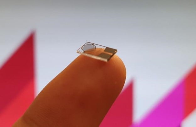


Researchers from NIMS and the Tokyo University of Science claim that they have developed the fastest electric double-layer transistor using a highly ion conductive ceramic thin film and a diamond thin film. The transistor could be used to develop energy-efficient, high-speed, edge AI devices for applications including future event prediction and pattern recognition/determination in images (including facial recognition), voices, and odors. The research was published in Materials Today Advances.
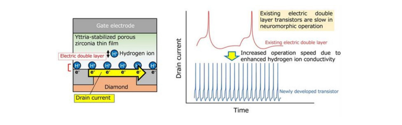
The electric double-layer transistor performs as a switch using electrical resistance changes caused by the charge and discharge of an electric double layer formed at the interface between the electrolyte and semiconductor. The transistor mimics the electrical response of human cerebral neurons, making its use in AI devices promising. Existing electric double-layer transistors are slow in switching between on and off, with speeds from several hundreds of microseconds to 10 milliseconds.
This team deposited ceramic and diamond thin films with high precision using a pulsed laser, forming an electric double layer at the ceramic/diamond interface. The zirconia thin film absorbs large amounts of water into its nanopores and allows hydrogen ions from the water to migrate through it. This enables the electric double layer to charge and discharge rapidly. The speed at which the transistor operates by applying a pulsed voltage was 8.5x faster than existing electric double-layer transistors, for a new world record. The team also confirmed the ability of this transistor to convert input waveforms into many different output waveforms with precision—a prerequisite for transistors to be compatible with neuromorphic AI devices.
This represents an important achievement in creating practical, high-speed, energy-efficient AI-assisted devices.