The integration of 2D materials into devices like computer chips is complicated. The ultrathin structures are easily damaged using conventional fabrication techniques that rely on chemicals, high temperatures, or etching. MIT researchers developed a method to integrate 2D materials in a single step while keeping the surfaces of the materials and the resulting interfaces free from defects.
They rely on engineering surface forces available at the nanoscale, allowing 2D material to be physically stacked onto other prebuilt device layers. Since the 2D material remains undamaged, they can take full advantage of its unique optical and electrical properties.
The approach was used to fabricate arrays of 2D transistors that achieved new functionalities compared to devices produced using conventional fabrication techniques. Their method is versatile enough for many materials and diverse high-performance computing, sensing, and flexible electronics applications. Central is the ability to form clean interfaces held together by van der Waals forces.

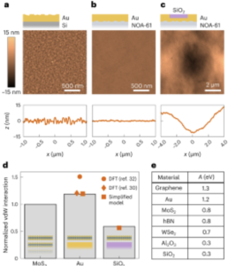
Van der Waals integration, unfortunately, has a fundamental limit. The forces depend on the intrinsic properties of materials and cannot be readily tuned. Some materials, therefore, cannot be directly integrated using their van der Waals interactions alone. The team created a platform to help make integration more versatile and promote the development of 2D-materials-based devices with new and improved functionalities.
The researchers focused on building devices and systems from the bottom up, using 2D materials and a process that requires sequential physical stacking. Rather than using chemical glues or high temperatures to bond a fragile 2D material to a conventional surface like silicon, they leverage van der Waals forces to physically integrate a layer of 2D material onto a device.
They form a hybrid surface of metals and insulators on a carrier substrate to make electronic devices. The cover is then peeled off and flipped over to reveal a smooth top surface containing the desired device’s building blocks. Then, the researchers prepare the 2D material separately in a spotless environment and bring it into direct contact with the prepared device stack, and integrate it with the surface. This process keeps the 2D material interface completely clean, which enables the material to reach its fundamental limits of performance without being held back by defects or contamination.