Moore’s Law predicted that the number of transistors on a chip would double every two years. Limitations exist. Today’s advanced chips can house nearly 50 billion transistors in a thumbnail’s space. Packing more in is more than problematic. However, a study by Penn State published in the journal Nature proposes seamlessly implementing 3D integration with 2D materials.

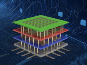
3D integration, or the vertical stacking of multiple layers of semiconductor devices, facilitates the packing of more silicon-based transistors onto a computer chip. This is commonly referred to as “More Moore” and permits using transistors made from 2D materials for diverse functionalities within various stack layers, a concept known as “More than Moore.”
Monolithic 3D integration offers the highest density of vertical connections, providing more space to make connections.
A challenge is the process temperature ceiling of 450 C for back-end integration for silicon-based chips. Monolithic 3D integration drops that temperate to less than 200 C. 2D materials can withstand the temperatures of the process.
By decreasing the distance between devices, the team reached “More Moore.” And, by incorporating transistors made with 2D materials, they met the “More than Moore” criterion.’ More Than Moore results in computer chips that are smaller and faster, but also have more functionalities. It includes adding new features to electronic devices, including better sensors and improved battery management.
The study demonstrated 3D integration at a massive scale, characterizing tens of thousands of devices, bridging the gap between academia and industry, and could lead to future partnerships leveraging Penn State’s 2D materials expertise and facilities.
The team put 30,000 transistors in each tier, which may be a record number. Penn State is uniquely positioned to partner with the U.S. semiconductor industry in advancing this research.