The landmarks set by the International Technology Roadmap for Semiconductors (ITRS) don’t always happen on their predicted dates. For instance, the ITRS predicted that by 2015, copper-based vias that connect the silicon surface to a chip’s wiring and connect one layer of wiring to another simply would not be able to do the job anymore.
Well, copper-based vias and interconnects are still with us. However, investigators believe it’s not too early to think about what should come next.
Kaustav Banerjee, a professor at the University of California-Santa Barbara, is one of the world’s leading researchers exploring the use of carbon-based nanomaterials to replace copper in electronic chip interconnects. We reported on his team’s investigation back in 2013 into making an entire chip, including interconnects, out of a single layer of graphene.
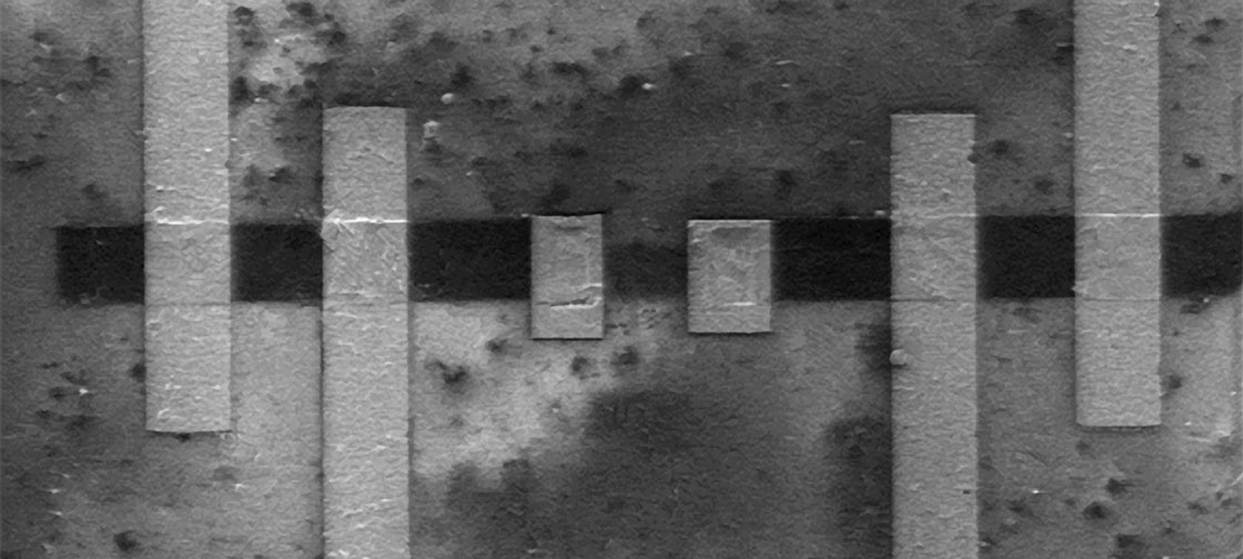
While Banerjee characterizes their previous graphene research from 2013 as more of a “radical idea,” he and his team reported far more practical work last week at the IEEE International Electron Devices Meeting (IEDM). They introduced an ‘all-carbon’ interconnect technology—comprised of multilayer-graphene wires and carbon nanotube vias—to improve performance and reliability while reducing energy consumption compared to copper interconnects for sub-10 nanometer nodes.
Banerjee points out that the ITRS projections for the phasing out of copper interconnects may have been a bit aggressive. He points out that, at present, the minimum line widths are around 26 to 30nm.
“We will start seeing serious problems with copper once we scale below 20 or 15nm,” said Banerjee. “That is when we should see some ‘carbon-based interconnects,’ at least at the local levels that use the most aggressive line widths.”
This latest effort reported at the IEDM conference builds on previous work that Banerjee and his team reported in the journal Nano Letters at the beginning of 2017. In that breakthrough research, Banerjee and his group members employed a process known as intercalation, which involves the inclusion of a molecule or ions between two other molecules in multilayered structures or compounds. In this case, the intercalation was used with multilayer graphene nanoribbons (ML-GNRs).
What the researchers found at the time was that these ML-GNRs provided better performance, reliability, and energy efficiency down to 20nm widths than copper interconnects.
The new research reported at IEDM advances this previous work by addressing one of the key integration challenges related to the graphene interconnect technology, according to Banerjee.
“The key issues at this moment are mostly related to processing/engineering,” said Banerjee. “We are working with some industry partners to make the doped-multi-layer graphene interconnects compatible with CMOS Back-End-Of-Line (BEOL) technology.”
Banerjee adds that he and his team have already developed “suitable carbon-based” vias that connect adjacent interconnect layers, which represent an essential part of the overall interconnect technology development, as reported in their IEDM paper.
The main focus of their continued work with these graphene-based interconnects is to address their compatibility with CMOS and BEOL process engineering. Specifically, Banerjee explained that this will involve developing controlled synthesis or transfer of wafer-scale multi-layer graphene on dielectric substrates at BEOL compatible temperatures (< 450°C). All of this will also require further modeling of multilayer-graphene interconnects and carbon-based vias for circuit-level analysis.