


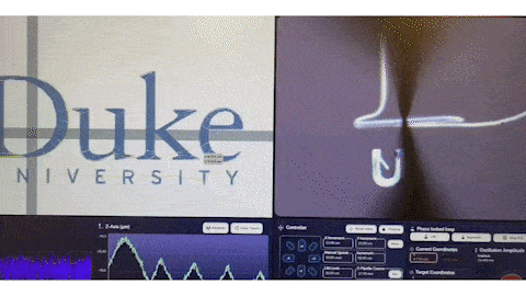
A team at Duke University has demonstrated a high-precision printing method that can fabricate thin-film transistors with features below one micrometer, using materials that are fully recyclable. The work targets one of the most resource-intensive sectors in electronics manufacturing: display backplanes.
Today’s flat-panel displays rely on thin-film transistors built using vacuum deposition and photolithography. These processes demand high energy input, require specialized facilities that are largely overseas, and generate significant waste. Once displays reach end of life, their device layers are difficult to disassemble, and the materials are rarely recovered.
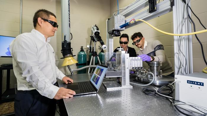
The Duke researchers worked with a printing system developed by Hummink that uses capillary flow to form extremely fine lines of ink. Instead of forcing material through a nozzle, the system uses a pipette tip and surface tension to draw the ink onto the substrate. This approach allows for precise deposition without the clogging and directional limitations of conventional printed electronics.
Using carbon-based inks, the team printed transistor structures with channel lengths below one micrometer. The inks can be applied to both rigid substrates like silicon and to recyclable or biodegradable platforms. After printing, the devices demonstrated electrical performance levels suitable for use in display-driving circuitry, where moderate switching speeds and large-area uniformity are more important than nanometer-scale dimensions.
One of the most significant aspects of the work is that the printed components can be recycled. The inks and substrates can be separated and reused rather than being permanently bonded into a waste stream. This recyclability offers a potential path toward displays and sensor systems that are easier to reclaim after use.
The printing method eliminates high-temperature steps and complex transfer processes, which may reduce both manufacturing energy consumption and production cost if brought to scale. It also opens the possibility of producing electronics locally, rather than relying exclusively on offshore fabrication infrastructure.
While there is more work needed to address long-term device stability, environmental durability, yield across large areas, and integration into commercial manufacturing lines, the approach represents a scalable alternative to current TFT production. If further developed, it could change how display backplanes, flexible sensors, and large-area electronics are manufactured and retired.
Instead of accepting that electronics must be difficult to recycle, this work introduces a fabrication process that treats recyclability as a design requirement from the start.