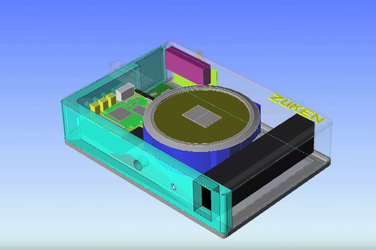


This DA14580 basic development kit from Dialog Semiconductor gives you all flexibility to develop with confidence. All of the DA14580’s I/Os are available and mapped on to expansion connectors. A debugger is provided on the PCB which in combination with SmartSnippets, Dialog’s complete software environment, enables you to program and test your applications.
- What is the DA14580 Development Kit for? Developing Bluetooth applications.
- How much does the DA14580 Development Kit cost? Currently available at $39.57.
- What’s in the box? Board, battery, USB cable and quickstart guide.
Tech Specs of the DA14580 Development Kit
| Processing power | 16MHz 32bit ARM Cortex-M0 with SWD interface, dedicated link layer processor, AES-128 bit encryption processor |
| Memories | 32kB One-Time-Programmable (OTP) memory, 42kB System SRAM, 84kB ROM, 8kB Retention SRAM |
| Power management | Integrated Buck/Boost DC/DC converter, P0, P1, P2 and P3 ports with 3.3V tolerance, easy decoupling of only four supply pins, supports coin (typ. 3.0V) and alkaline (typ. 1.5V) battery cells, 10-bit ADC for battery voltage measurement |
| Digital controlled oscillators | 16MHz crystal (±20ppm max) and RC oscillator, 32kHz crystal (±50ppm, ±500ppm max) and RCX oscillator |
| Digital interfaces | General purpose I/Os: 14 (WLCSP34 package), 24 (QFN40 package), 32 (QFN48 package), 2 UARTs with hardware flow control up to 1MBd, SPI+ interface, I2C bus at 100kHz, 400kHz, 3-axes capable Quadrature Decoder |
| Analog interfaces | 4-channel 10-bit ADC |
| Radio transceiver | Fully integrated 2.4GHz, CMOS transceiver, single wire antenna: no RF matching or RX/TX switching required, supply current at VBAT3V: TX: 3.4mA, RX: 3.7mA (with ideal DC/DC), 0dBm transmit output power, -20dBm output power in ‘Near Field Mode’, -93dBm receiver sensitivity |
| Packages | WLCSP 34 pins, 2.436×2.436mm; QFN 40 pins, 5x5mm; QFN 48 pins, 6x6mm;KGD (wafer, dice) |
Documentation
- [download id=”20214″]
- [download id=”20216″]