While Moore’s Law, which projected doubling the number of components per integrated circuit every two years, no longer really describes the state of the industry, it’s true that for decades, the transistors on our microchips have become smaller, faster and cheaper. Miniaturization has reached a natural limit, as completely new problems arise when a length scale of only a few nanometers is approached.
Now, however, the next big miniaturization step could soon become possible with so-called “two-dimensional (2D) materials” that may consist of only a single atomic layer. With the help of a novel insulator made of calcium fluoride, scientists at TU Wien (Vienna) have created an ultra-thin transistor, which has excellent electrical properties and, in contrast to previous technologies, can be miniaturized to an extremely small size. The new technology has now been presented in the journal Nature Electronics.
Ultra-Thin Semiconductors and Insulators
Research on semiconductor materials needed to fabricate transistors has seen significant progress in recent years. Today, ultra-thin semiconductors can be made of 2D materials, consisting of only a few atomic layers. “But this is not enough to build an extremely small transistor,” says Professor Tibor Grasser from the Institute of Microelectronics at TU Wien. “In addition to the ultra-thin semiconductor, we also need an ultra-thin insulator.”
This is due to the fundamental design structure of a transistor: current can flow from one side of the transistor to the other, but only if a voltage is applied in the middle, creating an electric field. The electrode providing this field must be electrically insulated from the semiconductor itself. “There have already been transistor experiments with ultra-thin semiconductors, but until now they were coupled with ordinary insulators,” says Tibor Grasser. “There is not much benefit in reducing the thickness of the semiconductor when it still has to be combined with a thick layer of insulator material. There is no way of miniaturizing such a transistor any further. Also, at very small length scales the insulator surface turned out to disturb the electronic properties of the semiconductor.”
Therefore, Yury Illarionov, a postdoc in Tibor Grasser’s team, tried a novel approach. He used ultra-thin 2D-materials not only for the semiconductor part of the transistor but also for the insulating part. By selecting ultra-thin insulating materials such as ionic crystals, a transistor with a size of only a few nanometers can be built. The electronic properties are improved because ionic crystals can have a perfectly regular surface, without a single atom protruding from the surface, which could disturb the electric field.
“Conventional materials have covalent bonds in the third dimension—atoms that couple to the neighboring materials above and below,” said Grasser. “This is not the case in 2D materials and ionic crystals, and so they do not interfere with the electrical properties of the semiconductor.”
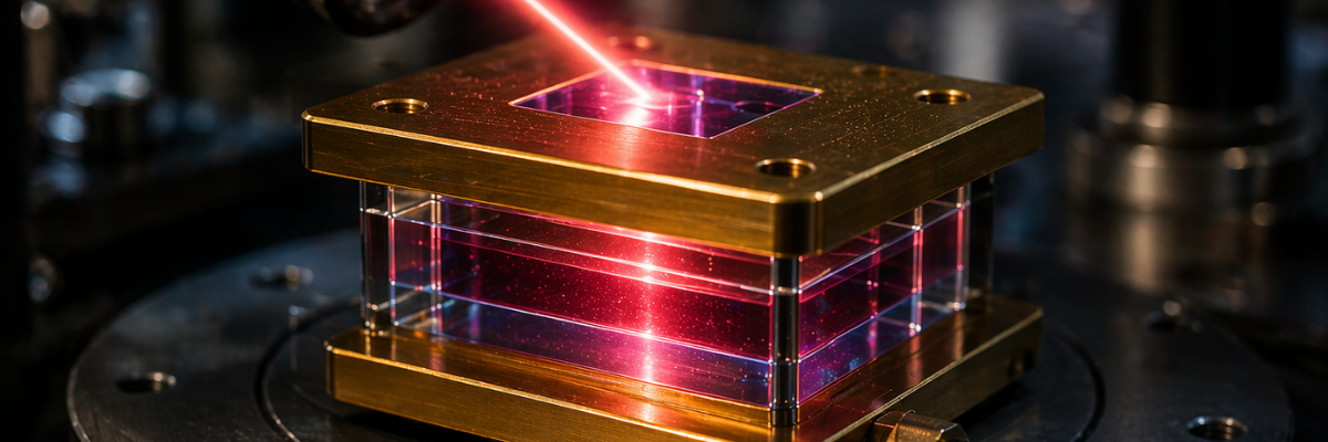
To produce the new ultra-thin transistor, calcium fluoride was selected as the insulating material, and the first prototype surpassed all expectations: “For years, we have received quite a number of different transistors to investigate their technical properties – but we have never seen anything like our transistor with the calcium fluoride insulator,” says Grasser. “The prototype with its superior electrical properties outshines all previous models.”
Now the team wants to find out which combinations of insulators and semiconductors work best. It may take a few more years before the technology can be used for commercially available computer chips as the manufacturing processes for the material layers still need to be improved. “In general, however, there is no doubt that transistors made of 2D materials are a highly interesting option for the future,” said Grasser. “From a scientific point of view, it is clear that the fluorides we have just tested are currently the best solution for the insulator problem. Now, only a few technical questions remain to be answered. ”
Source: Vienna Institute of Technology


