
 Toshiba Memory Europe
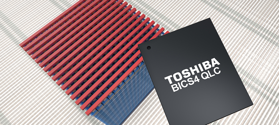
96-layer BiCS FLASH development with QLC technology
Toshiba Memory Europe has announced that it has developed a prototype sample of a 96-layer BiCS FLASH, memory device using its proprietary 3D flash quad level cell (QLC) technology that boosts single-chip memory capacity.
QLC technology is pushing the bit count for data per memory cell from three to four, expanding capacity. The new product achieves the industry’s maximum capacity of 1.33Tb for a single chip and was jointly developed with Western Digital.
This also realizes a capacity of 2.66Tb in a single package by utilizing a 16-chip stacked architecture. The volumes of data generated by mobile terminals and the like continue to increase with the spread of SNS and the progress in IoT and the demand for analyzing and utilizing that data in real time is expected to increase dramatically. This will require even faster HDDs and larger capacity storage and such QLC-based products, using the 96-layer process, will contribute to the solution.
Toshiba Memory will start to deliver samples to SSD and SSD controller manufacturers for evaluation from the beginning of September and expects to start mass production in 2019. A packaged prototype of the new device will be exhibited at the 2018 Flash Memory Summit in Santa Clara, California, USA from 6th to 9th August.