


Researchers from the University of Hamburg and DESY have developed a 3D printing process that can be used to produce transparent and mechanically flexible electronic circuits. The electronics consist of a mesh of silver nanowires that can be printed in suspension and embedded in various flexible and transparent plastics (polymers). This technology can enable new applications such as printable light-emitting diodes, solar cells or tools with integrated circuits,
“The aim of this study was to functionalize 3D-printable polymers for different applications,” said Michael Rübhausen from the Center for Free-Electron Laser Science (CFEL), a cooperation between DESY, the University of Hamburg and the Max Planck Society.
The overall goal of the project was to integrate electronics into existing structural units and improve components in terms of space and weight.
“At the heart of the technology are silver nanowires, which form a conductive mesh,” said Tomke Glier, from the University of Hambur, who led the project. The silver wires are typically several tens of nanometers (millionths of a millimeter) thick and 10 to 20 micrometers (thousandths of a millimeter) long. The detailed X-ray analysis shows that the structure of the nanowires in the polymer is not changed, but that the conductivity of the mesh even improves thanks to the compression by the polymer, as the polymer contracts during the curing process.
The silver nanowires are applied to a substrate in suspension and dried.
“For cost reasons, the aim is to achieve the highest possible conductivity with as few nanowires as possible. This also increases the transparency of the material,” explains Roth, head of the P03 measuring station at DESY’s X-ray light source PETRA III, where the X-ray investigations took place. “In this way, layer by layer, a conductive path or surface can be produced.” A flexible polymer is applied to the conductive tracks, which in turn can be covered with conductive tracks and contacts. Depending on the geometry and material used, various electronic components can be printed in this way.
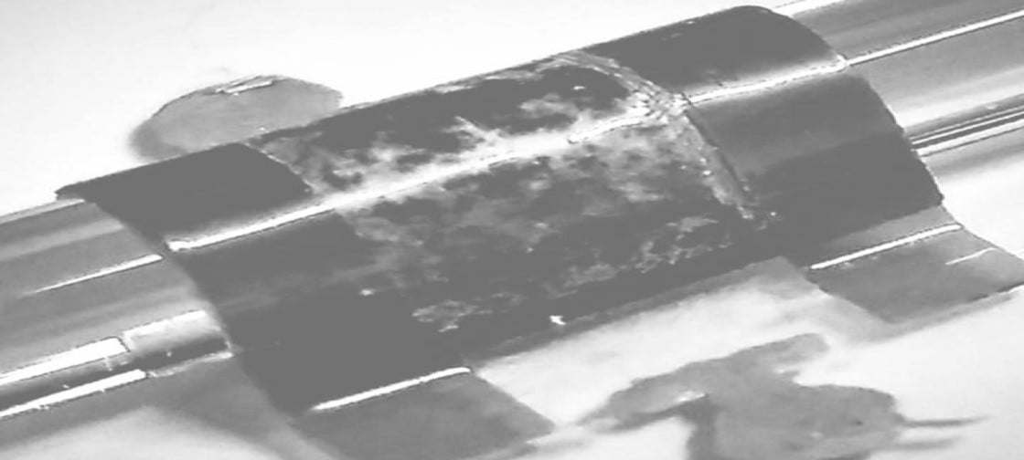
The researchers were able to produce a flexible capacitor via individual work steps in a layering process, but in practice, they would be completely transferred to a 3D printer. In order to successfully do this in the future, conventional 3D printing tech needs to be optimized for individual printing inks. In inkjet-based processes, the print nozzles could be clogged by the nanostructures.
In the next step, the researchers will test how the structure of the conductive paths made of nanowires changes under mechanical stress.
“How well does the wire mesh hold together during bending? How stable does the polymer remain?” asks Roth. “X-ray investigation is very suitable for this because it is the only way we can look into the material and analyze the conductive paths and surfaces of the nanowires.”
Story via University of Hamburg