For the past few years, engineers have modified the properties of some 2D materials that are one or a few atoms thick, by stacking two layers together and rotating one relative to the other, creating moiré patterns. This changes how electrons move through the material in potentially beneficial ways. However, when 2D materials must connect with 3D materials at the interface down to the level of individual atoms and correlate the moiré patterns at the 2D-3D boundary, complexity occurs.
A paper by MIT graduate students Kate Reidy and Georgios Varnavides, professors of materials science and engineering Frances Ross, Jim LeBeau, and Polina Anikeeva, and five others at MIT, Harvard University, and the University of Victoria in Canada describes new findings in Nature Communications journal.
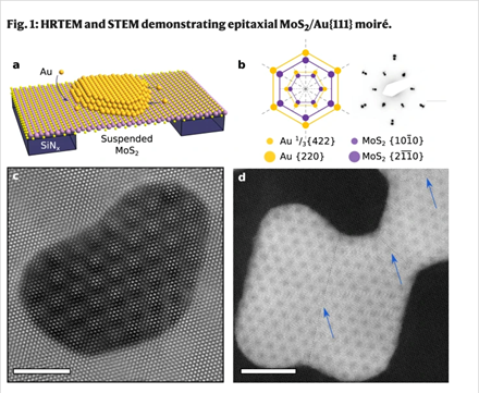
The research team addressed that little is known about what happens where 2D materials meet regular 3D solids. It was a daunting challenge given that electron microscopes produce an image of the sample in projection and are limited in their ability to extract the depth of information needed to analyze details of the interface structure. The team created a set of algorithms to extrapolate back from images of the sample, which look somewhat like a set of overlapping shadows, to figure out which configuration of stacked layers would yield a complex “shadow.”
Unlike stacked 2D materials, where orientations are easily changed, the bonds holding 3D materials together are much stronger. They added the 3D material onto the 2D material in ultrahigh vacuum, choosing growth conditions where the layers self-assembled in a reproducible orientation with specific degrees of twist. A scanning transmission electron microscope actually produced more information than did a flat image. The data can be separated out so that the information at all points in an image can be used to decode the actual solid structure.
The researchers used such techniques as 4D STEM and an integrated differential phase contrast to achieve that process of extracting the full structure at the interface from the image and showed through modeling that electronic properties are expected to be modified in a way that can only be understood if the full structure of the interface is included in the physical theory
The paper can be found at: Direct imaging and electronic structure modulation of moiré superlattices at the 2D/3D interface.