Among the first to produce a single, three-atom-thick layer of an exceptional 2D material called tungsten ditelluride, the researchers at the University of Pennsylvania, have had their findings published in 2-D Materials.
Unlike other 2D materials, scientists believe tungsten ditelluride has what are called topological electronic states. This means that it can have many different properties not just one.
Graphene normally springs to mind first when you think about 2D materials.
The tightly packed, atomically thin sheet of carbon first produced in 2004 has inspired countless avenues in research that could revolutionize everything from technology to drinking water.
One of the most important properties of graphene is that it’s what’s called a zero bandgap semiconductor in that it can behave as both a metal and a semiconductor.
But there are tons of other properties that 2D materials can have. Some can insulate, others can emit light and still others can be spintronic, meaning they have magnetic properties.
“Graphene is just graphene,” said A.T. Charlie Johnson, a Physics Professor in Penn’s School of Arts & Sciences. “It just does what graphene does. If you want to have functioning systems that are based on 2D materials, then you want 2D materials that have all of the different physical properties that we know about.”
The ability of 2D materials to have topological electronic states is a phenomenon that was pioneered by Charles Kane, the Christopher H. Browne Distinguished Professor of Physics at Penn.
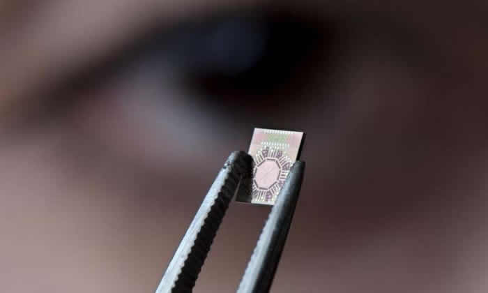
In this new research, Johnson, physics professor James Kikkawa and graduate students Carl Naylor and William Parkin were able to produce and measure the properties of a single layer of tungsten ditelluride.
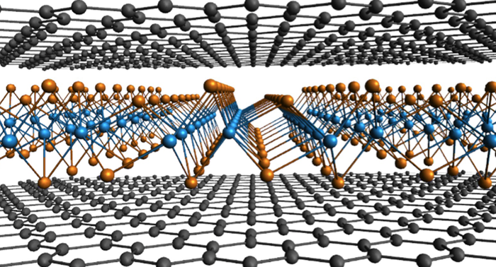
“Because tungsten ditelluride is three atoms thick, the atoms can be arranged in different ways,” Johnson said. “These three atoms can take on slightly different configurations with respect to each other. One configuration is predicted to give these topological properties.”
“It’s very much a Penn product,” Johnson said. “We’re collaborating with multiple other faculty members who investigate the material in their own ways, and we brought it all together to put a paper out there. Everybody comes along for the ride.”
The researchers were able to grow this material using a process called chemical vapor deposition. Using a hot-tube furnace, they heated a chip containing tungsten to the right temperature and then introduced a vapor containing tellurium.
“Through good fortune and finding exactly the right conditions, these elements will chemically react and combine to form a monolayer, or three-atom-thick regions of this material,” Johnson said.
Although this material degrades extremely rapidly in air, Naylor, the paper’s first author, figured out ways to protect the material so that it could be studied before it was destroyed.
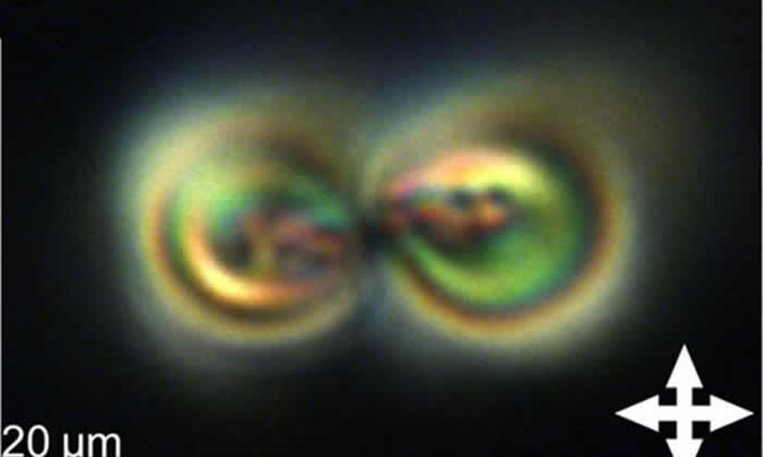
One thing the researchers found is that the material grows in little rectangular crystallites, rather than the triangles that other materials grow in.
“This reflects the rectangular symmetry in the material,” Johnson said. “They have a different structure so they tend to grow in different shapes.”
Although the research is still in its beginning stages and the researchers haven’t yet been able to produce a continuous film, they hope to conduct experiments to show that it has the topological electronic properties that are predicted.
One property of these topological systems is that any current traveling through the material would only be carried on the edges, and no current would travel through the center of the material. If researchers were able to produce single-layer-thick materials with this property, they may be able to route an electrical signal to go off into different locations.
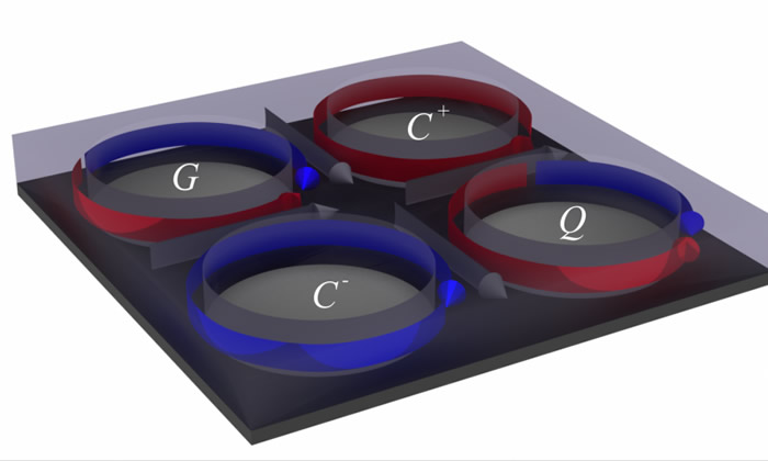
The ability of this material to have multiple properties could also have implications in quantum computing, which taps into the power of atoms and subatomic phenomena to perform calculations significantly faster than current computers. These 2D materials might allow for an intrinsically error-tolerant form of quantum computing called topologically protected quantum computing, which requires both semiconducting and superconducting materials.
Johnson added: “With these 2D materials, you want to realize as many physical properties as possible. Topological electronic states are interesting and they’re new and so a lot of people have been trying to realize them in a 2D material. We created the material where these are predicted to occur, so in that sense we’ve moved towards this very big goal in the field.”
More information: Phys.org