The Internet of Moving Things (IoMT) is here. From smartphones and tablets to smart clothing and wearables, everyday objects and devices are now able to measure, monitor and analyse motion, generating massive amounts of data and insight. We caught up with Ben Lee, CEO of MEMS sensor developer mCube, based in Silicon Valley, on what the company brings to the market space and an intriguing acquisition.
By 2020, analysts predict that more than 50 billion devices will be connected to the internet. A large percentage of those devices will be in motion or moving (the IoMT) and this is the focus for mCube. MEMS sensors will be pervasive in anything that moves and there are obvious applications for the IoMT such as wearables. However, there are many more applications to the IoMT than meet the eye.
For example, when mCube came up with what it claims is the world’s lowest power and smallest motion sensor, the company was targeting the activity market. However, the first design win was a door lock. “You may not think that a door is moving, but it actually is,” said mCube CEO Ben Lee. “Our sensor picks up the position of the lock so you can see on your phone whether the door is locked. You can also use your phone to lock and unlock the door. Even when the mechanism of the lock is not moving, when someone knocks on the door our sensors pick up the vibration and sends a message to your phone.”
mCube
Founded: 2009
Head office: San Jose, Ca.
141 patents filed
Over 300Mu shipped
mCube also has a customer in Japan that is working on a sensor chip that goes on a pipe. Lee added: “Again you may not think a pipe is moving. Japan however, is a very seismic place, so it’s important to know the level of motion during seismic activity, but more importantly, to know the position of the pipe afterwards. So, if the pipe has tilted more than a few degrees it puts huge pressure on the joints which can cause leaks. So this customer has a project to put battery powered sensors on infrastructure next to every building that will last ten years. When the stresses reach a certain level it will transmit a message to the operator to say ‘come and fix me’. This is a huge market in terms of smart cities.
“We hadn’t classified these types of application previously as IoMT, so it’s a much bigger part of the IoT than we originally thought.”
What mCube offer
mCube offers monolithic MEMS+CMOS motion sensors to mass volume production. The company claim that monolithic MEMS accelerometers enjoy substantial size, cost, power and performance advantages over the multi-chip modules from competing MEMS sensor manufacturers.
With the mCube approach, MEMS sensors are fabricated directly on top of the IC electronics in a standard CMOS fabrication facility. Advantages of this monolithic approach include smaller size, higher performance, lower cost. Plus the ability to integrate multiple sensors onto a single chip.
MEMS technology is very difficult and is described by Lee as being akin to black magic or a combination of art and science. He said: “Traditional electronic component foundries have very clear design rules. If followed, they will produce a working chip at the end. MEMS is not defined in this way however. It’s a mechanical device so creating it is a little bit like art, and there’s a lot of know-how required. Anyone can carve one out, but can you ship 300 million units that are all the same? Many PHDs students have done MEMS projects, and I interview hundreds. But as soon as I ask how many have you shipped, the interview tends to stop, because there are very few companies that can deal with this sort of volume.”
Don’t just take my word for it, was Lee’s message as he highlighted a 2015 comparison report from SYSTEMPlus on what they thought were the three leading MEMS accelerometers. He added: “They got samples, decapped them and they were shocked.”
Leading MEMS accelerometers comparison
On the outside the accelerometers appeared the same. However, when they looked inside they found two different chips, one an ASIC and one the mechanical moving part, bonded together using gold wires. Lee added that every MEMS company in the world employs this approach of using two different dies bonded together.
“We don’t have these wires as we only have one piece of die,” he continued. “SystemPlus call it disruptive technology and it has a variety of advantages. For example, fewer bonding wires means better reliability and lower assembly costs. The other MEMS guys ship two wafers. They build their MEMS wafer in one factory, their CMOS in another. The two are then shipped to the assembly house who then stack them and wire bond them. We ship one wafer which is a much more streamlined process. This also leads to higher performance – for two reasons. Number one is that we all know that when you try and transmit a very small signal through many different materials, you will lose the power of the signal. We obviously don’t have that so the signal we get for the ASIC is very high quality.
“Secondly, because there is a moving part inside the sensor, it is being sensed by capacitance change relative to the sensor. So you want to have a lot of sensing elements around the part to track its movement. Every sensing element needs a wire to transmit the signal to the ASIC. However, due to space constraints the other guys can’t fit that many in leading to reduced performance.
Size matters
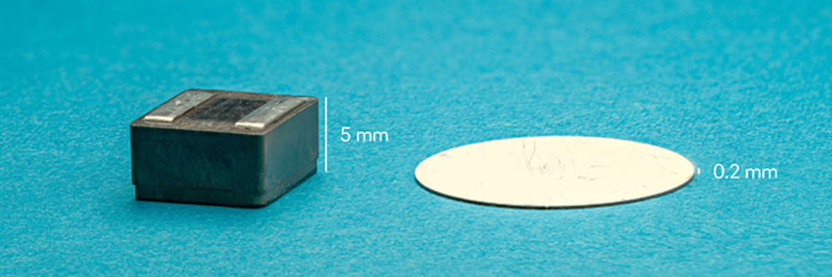
“Our MC3672 accelerometer is 1×1 x 3×0.74mm which no one is able to match. As a matter of fact, we’ve been doing this since 2010 and to this day, no one else has done it. The reason is that competitors tend to have a separate factory for MEMS and a separate factory for CMOS.
“We do it all in one factory. So even if they decide to rebuild their infrastructure, that’s when they would encounter the 100 plus patents we have on our technology, but they haven’t even done that step as it’s too expensive.”
Lee continued: “We took the world’s only chip scale accelerometers from mCube, and took our nearest competitor’s reference board and put them next to each other. Looking at this our marketing guys have a very easy job. They show this to our customers and ask whether they’d like to use the one on the left or the one on the right? However, the most important question is what designs were they not able to do before because of size constraints? Our accelerometer is 89% smaller than our nearest competitor.” Lee claims that this size reduction will open up the miniaturisation of electronics so technology itself will start to disappear.
“Our accelerometer is 89% smaller than our nearest competitor.”
Rapidly bringing IoMT to life
With the aim of sparking a new wave of innovation for the IoMT, mCube has acquired Netherlands-based Xsens, an expert in sensor fusion. By combining the two companies, mCube expects create new markets for motion sensing and tracking solutions. Working alongside Xsens’s experts in sensor fusion and motion tracking modules, mCube hope to enable its customers to develop motion enabled applications faster by taking the complexity out of MEMS sensors with highly integrated solutions.
“Xsens produce the world’s leading sensor fusion software”, added Lee. “We believe that sensor fusion will become more and more critical for motion tracking applications in IoMT. Sensors come in a number of different variations – gyroscopes, accelerometers, barometers etc all measuring different parameters. Xsens coordinates all this information into data that an application can understand – this is called sensor fusion. And this is why Xsens and mCube are a perfect fit. No other company has a combination like Xsens’ sensor fusion technology and our leading edge MEMS sensor technology.
“They’ve been around since 2000 and have acquired a lot of sensor fusion know-how. The difference between them and other sensor fusion companies, and there are others around, is that most companies licence their sensor fusion software to hardware companies. That’s not the way Xsens work. They use their software to build embedded plug-and-play modules to various end customer applications.”
Why Xsens? Why now?
Xsens were acquired by Fairchild in 2014 after eyeing its sensor fusion software. Then, following ON Semiconductor’s acquisition of Fairchild, it was decided that it was not part of its core business. So ON Semiconductor surveyed the market for a good home for xSens. They then determined that mCube was the best match.
Why is this a good fit for mCube? Lee added: “We find that in IoT a lot of customers need help with a solution. Sensor companies can no longer just sell a sensor because a lot of these customers don’t know how to use it. They are simply not historically involved in electronics. So they are asking us to develop algorithms to put on the processor. To run the algorithms and put it together in one package. Before you know it, we’re designing the whole thing. We can do this but there’s more value in the subsystems.
A perfect fit
“So mCube was already on this path to provide solutions on top of our sensors. But that is exactly the business of xSens. They don’t make the sensors but they are the masters of sensor fusion in their modules. It would take us years to get there just by ourselves. So with the acquisition it really speeds up our path to providing total solutions to the IoT world.
“That is the biggest benefit. A secondary benefit is that when we define and develop a new sensor we go around and ask customers what their required specification is. Ten customers will give you ten different answers and you then have to try and meet the most needs possible. Because Xsens are involved in all these different applications, they can tell us how to spec our next chip. This is very advantageous and speeds up our time to market. And we can use the sensor fusion to accelerate our path to total solutions.
“You won’t be able to just provide a sensor in the future, you’ll have to provide solutions. Everyone is trying to do this, but by acquiring xSens we have taken a huge leap forward.
“In the future everything will have sensors in it and you won’t even know. But it will help you in your everyday life.”
“What do xSens get out of it? Well that’s where our miniaturisation comes in. We can make their sensor fusion even smaller so in the future the technology will just disappear. Wearables will be truly wearable. For example, you’ll buy a jacket with 20 sensors on it. You’ll wear it, wash it, and throw it away and you’ll never know the technology was there at all. Just like a car today. An average car has around 200 sensors on it. If I was to ask someone where they are, they wouldn’t be able to point them out. However, they’ll drive the car in the same way as they drove an old car without any electronics. Clothing will be the same. In the future everything will have sensors in it and you won’t even know. But it will help you in your everyday life.


