At this week’s 2017 International Electron Devices Meeting (IEDM), imec presented the first Power-Performance-Area-Cost (PPAC) analysis of different sequential 3D-integration variants using advanced 5 and 3nm CMOS technology nodes.
The most significant benefit was found for a heterogeneous sequential-3D integration approach that uses different device layers (or tiers) for the non-scalable (analog and I/O) and scalable parts (logic and memory) of the system. These results confirm the potential of heterogeneous sequential-3D integration as a possible route for heterogeneous scaling—an emerging approach that integrates multiple transistor architectures in one system-on-chip.
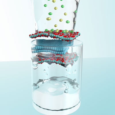
Sequential-3D integration (S3D) is widely viewed as a promising alternative to continue the benefits offered by semiconductor scaling.
S3D involves the vertical integration of sequentially processed device layers (or tiers) with isolation and interconnect layers in between.
Three levels of granularity can be defined, depending on where the partitioning and stacking takes place: at the transistor level (T-S3D), cell level (C-S3D) or IP block level, also called heterogeneous S3D (H-S3D). H-S3D is considered as a possible enabler for heterogeneous scaling. Compared with traditional through-Si-via (TSV)-based 3D-integration techniques, S3D in general offers a higher interconnect density and a more precise (lithography-defined) alignment of the stacked transistors, cells and IP blocks.
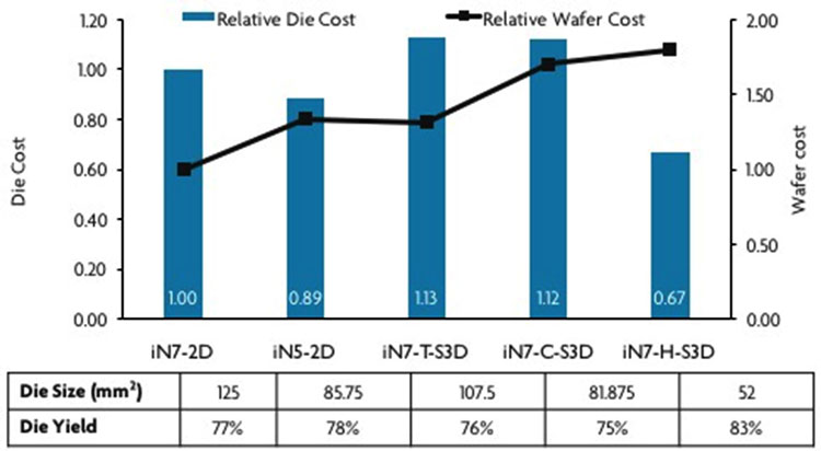
For the first time ever, imec has quantified the power-performance-area-cost (PPAC) benefits of the various S3D variants for 5 and 3nm technology nodes. To meet the challenges for S3D fabrication, the imec team used advanced technologies in some of the most critical process steps. The largest PPAC benefit was found for a heterogenous S3D use case, where the logic and memory part is scaled to iN5 technology, and the remaining non-scalable part (analog and I/O) is manufactured in N28 technology in the top tier. For this use case, despite a high wafer cost, a die cost reduction of 33% was achieved with respect to a 2D-SoC implementation with 125mm2 die size.
“Our results demonstrate the potential of S3D technology which benefits the implementation of next-generation application hardware such as 5G and Artifical Intelligence,” stated Nadine Collaert, distinguished member of the technical staff at imec.
Imec’s research into advanced logic scaling is performed in cooperation with imec’s key CMOS program partners including GlobalFoundries, Huawei, Intel, Micron, Qualcomm, Samsung, SanDisk/Western Digital, SK Hynix, Sony Semiconductor Solutions, TOSHIBA Memory and TSMC.