


Nowadays, there is broad consensus in the memory industry that the 28nm/22nm silicon lithography nodes will be the last technology nodes for eFlash. This is not because of fundamental scalability limitations, but because of economic barriers. Therefore a new embedded NVM for code/data storage is needed.
At the same time, scaling of volatile SRAM is slowing down due to cell footprint degradation occurring at advanced nodes. A denser working embedded memory would therefore be highly desirable.
Thanks to the support of a large number of leading companies, the embedded memory market has the potential to reach $1.2bn by 2024, growing with a 295% CAGR over this period. In parallel, the stand-alone (STT-)MRAM market is expected to grow less vigorously than its embedded counterpart, with revenues up to about $580m in 2024, announces Yole in its latest MRAM Technology and Business report, released last week and presented at the MRAM Developer Day this week in Santa Clara. Simone Bertozzi had the opportunity to present the latest technology trends and a relevant market update to the memory community.
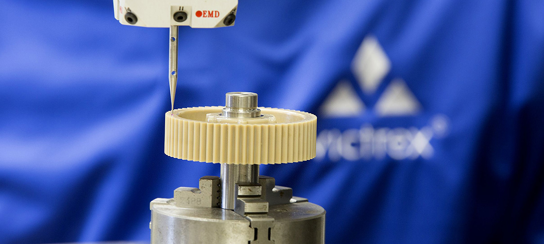
MRAM promises life beyond eFlash: the embedded MRAM market is taking off. Yole & System Plus Consulting memory team offers you today a relevant snapshot.
Among various emerging NVM technologies, spin transfer torque magnetoresistive RAM (STT-MRAM) is gaining significant momentum. It is poised to become the next embedded memory solution for a variety of IC products manufactured at the 28nm node and below. That includes low-power wearables and IoT devices, MCUs, automotive, imaging and display ICs, edge AI accelerators, and other ASICs and ASSPs.
“In 2018, the embedded STT-MRAM market was still limited, with no volume shipments”, explained Simone Bertolazzi from Yole. “2019 is expected to be the year this market takes off. Samsung has recently started mass production of embedded STT-MRAM, and Yole expects other major foundry/IDMs to enter the race soon.”
At the same time, multiple equipment suppliers like Applied Materials, Tokyo Electron Limited (TEL), Canon, and Lam Research, and logic companies like Qualcomm, ARM and Synopsis are increasing their research spending on MRAM. This is further propelling the development of the embedded STT-MRAM business.
On the other hand, the stand-alone memory market is expected to grow less vigorously, with a 54% CAGR between 2018 and 2024. According to Yole’s analysts, it will remain below $600m in 2024. So far, the growth has been driven by low-density (STT-)MRAM devices at 16Mb and below manufactured by a few key players, such as Everspin and Avalanche/Sony.
In coming years, the stand-alone market will be mainly driven by enterprise storage applications. These include SSD caching and storage/network accelerators, which are served by high-density STT-MRAM chips at 256Mb and above. The latter are typically sold to IDMs and system makers in the enterprise storage business. These companies require 12 to 18 months to develop new systems, so the ramp-up of STT-MRAM sales has taken a relatively long time.
Notably, 1Gb 28nm devices from Everspin have recently moved into the pilot-production phase at GlobalFoundries. Their forthcoming availability in the market could trigger further growth of enterprise storage applications. Yole’s analysts had the opportunity to debate with Martin Mason, Senior Director of Embedded Memory at GlobalFoundries.
Mike Howard, VP of DRAM & Memory Research at Yole, commented: “DRAM consolidation took more than 30 years as new participants continually entered the market with the aid of IP from distressed suppliers and government-backed capital”, asserts. And he adds: “Prior to 2013, DRAM prices fell 75% of the time…since consolidation in 2013 they have only fallen 50% of the time.”
Walt Coon, VP of NAND & Memory research at Yole, added: “Over the past 2 decades, the NAND market has experienced tremendous growth but has been plagued by significant volatility and prolonged downturns.”
“NAND Manufacturers continue to meet the progressive demand of high-performing Flash memories with higher capacity by increasing the number of layers and reducing the die size,” said Belinda Dube, Cost Analyst at System Plus Consulting. “The recent generation allows manufacturers to produce increased Gigabytes per wafer. 3D technology continues to meet the market demands but the complexity of the 3D structure with added layers presents different manufacturing challenges. Future generations will see manufacturers altering their manufacturing process and memory design.”