
In a significant leap forward for optical technology, researchers have unveiled a new programmable photonic latch—a groundbreaking optical memory unit designed to enhance processing speed and energy efficiency in computational systems. This innovation promises to transform applications like artificial intelligence (AI), sensing, and other computation-intensive processes by integrating high-speed optical memory into silicon photonics.
Advancing Optical Memory Technology
The programmable photonic latch, developed by Farshid Ashtiani and his team at Nokia Bell Labs, is modeled after the widely used set-reset latch found in electronic devices. This new optical counterpart enables temporary data storage by switching between “set” (1) and “reset” (0) states. Unlike traditional electronic memory, this photonic solution allows optical processing systems to operate with improved efficiency and throughput, reducing energy consumption and latency.
“While optical communications and computing have advanced significantly, data storage has remained predominantly electronic,” said Ashtiani. “Integrating fast optical memory into optical processing systems would enhance energy efficiency and processing speeds for applications like AI and sensing.”
Scalable and Fast Optical Memory
One of the key breakthroughs of the photonic latch is its scalability. The memory units operate independently without affecting one another, thanks to dedicated input light sources. This makes it possible to create high-density memory configurations while maintaining reliability.
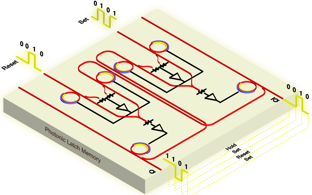
The photonic latch is also designed to work seamlessly with wavelength division multiplexing (WDM), which allows multiple data streams to be stored and retrieved simultaneously within a single unit. With response times measured in tens of picoseconds, this optical memory technology surpasses the clock speeds of even the most advanced digital systems.
Overcoming Challenges in Optical Data Storage
Until now, optical memory development faced challenges such as bulky, expensive setups and reliance on specialized materials not supported by standard silicon photonic fabrication processes. To address these issues, Ashtiani’s team built the programmable photonic latch using silicon photonic micro-ring modulators, which can be manufactured with existing commercial processes for higher yields and cost efficiency.
In proof-of-concept experiments, the researchers successfully demonstrated the functionality of the photonic latch, including optical set and reset operations, complementary outputs, and robust performance under varying input conditions.
Future Directions
The next steps for the research team involve scaling the technology to include a larger number of memory units and fabricating dedicated photonic memory chips. Integrating photonic memory circuits with the required electronic controls into a single manufacturing process will be critical for enabling higher memory densities and practical applications.
According to Ashtiani, this development is a pivotal step toward realizing commercial optical computers. “Our high-speed optical memory could enable much faster operations in systems like large language models, bridging the gap between optical data processing and storage.”
Impact on the Industry
Optical memory technologies like the programmable photonic latch are expected to have a transformative impact on industries ranging from telecommunications to AI. By addressing inefficiencies in optical-electronic data conversion, this innovation represents a significant milestone in the evolution of optical computing.
About Optica Publishing Group
The research is published in Optics Express, a peer-reviewed, open-access journal under the Optica Publishing Group. Optica is a leading global society dedicated to advancing optics and photonics. The full paper, “Programmable photonic latch memory,” by F. Ashtiani, provides detailed insights into this cutting-edge development.
For More Information
For additional details, visit Optics Express.