Introduction
Over the past decade, wide bandgap semiconductors have taken a strong foothold in power electronics applications across the power spectrum from consumer adapters and chargers and battery powered devices such as power tools to EVs and traction inverters for railway applications. Silicon carbide (SiC) MOSFETs in particular, offer high power densities with 650-V, 1200-V, and higher rated SiC FETs where higher switching frequencies allow for smaller passive device peripherals in the application circuit. The result: less power devices and smaller passives to achieve the same power capabilities.
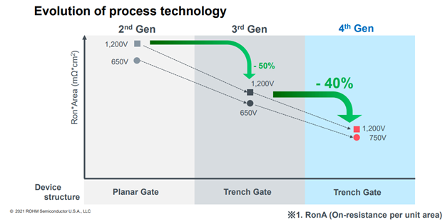
To take full advantage of the inherent benefits of the SiC substrate, it is critical to optimize both the on-state resistance (Ron) and gate charge (Qg) for lower conduction and switching losses. This is where steady improvements in the SiC process is key. ROHM’s breakthrough 3rd generation technology incorporated a novel trench gate structure to optimize transistor performance. This has been steadily improved with its 4th generation (4th gen) process.
However, the design problem does not end there. SiC packaging must contribute minimal parasitics to minimize losses; optimize its die-attach technologies to maximize thermal performance; assess wire bonding to withstand power cycling; and optimize package size to reduce PCB mounting area. For over 20 years, ROHM has developed SiC Schottky barrier diodes (SBDs) and MOSFETs with integrated production from up to 8” wafer fabrication to molded modules that are entirely SiC. This article discusses two specific molded modules—the HSDIP and DOT-247—their features, and their benefits for end-applications such as EVs and industrial power technologies.
ROHM’s SiC Process Innovations
As shown in Figure 1, ROHM’s power dense 4th generation SiC MOSFETs further optimize the double-trench structure allowing for a massive drop in Ron without sacrificing short circuit ruggedness, leading to much lower conduction losses. The technology also improves switching performance by ~50% thanks to a drastically reduced device capacitance. The improved switching with lower Crss/Ciss, in addition to a higher gate threshold voltage, mitigates the risk of self turn-on, and supports 15V~18V on-state bias with no need for negative voltages in turn-off.
Challenges: Packaging SiC Devices
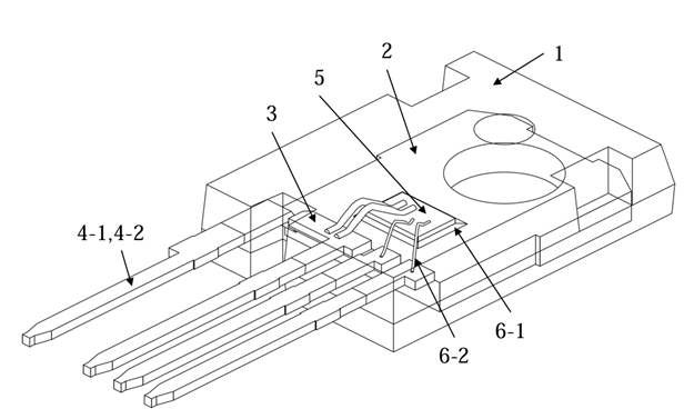
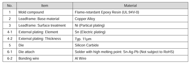
Increasing power output and miniaturization are both critical for the ongoing optimization of SiC power devices. The constant drive to improve current and power density within the same die size can only be taken advantage of with the right packaging technologies. Every aspect of the package must be optimized, from bond wires and die-attach technology; to the materials employed and built-in isolation. An example of the inner structure of the TO-247-4L package can be seen in Figure 2.
Parasitics
Bare die SiC will naturally have extremely low parasitic inductance on the order of ~1 fH that enables relatively unimpeded ultra-fast switching. However, the SiC-based converters will require packaging these power semiconductor devices that inevitably increases the internal and external parasitics such as stray inductance (and capacitance) found at the gate, drain, and source from bond wires and PCB interconnect. However, to achieve the inherently fast switching speeds of SiC, high frequency drives are required. The high dI/dt and dV/dt will interact with these parasitic components, and lead to unwanted overshoots and ringing. Typically, an external gate resistance is added to slow down the voltage and current (dI/dt and dV/dt). However, this leads to higher switching losses. Minimizing these package parasitics is key in taking advantage of a SiC FET’s switching capabilities. The TO-247-4L package shown in Figure 1, for instance, separates the driver and power source pins, minimizing the effects of the parasitic inductance component to maximize switching speed and reduce total switching losses.
Bond Wire and Die-Attach
Power electronics will experience high temperature differentials from turn-off to turn-on. High temperatures will cause expansions in various materials within the multi-layered package, each of which will expand and contract in accordance with its coefficient of thermal expansion (CTE). Thermal stress and failures generally occur at interfaces of materials with different CTEs where bond wires are often the weakest link in this chain. The highest mismatch is often found between the bond wires followed by the chip and solder layer [1]; improving the bond-wire and die-attach aspects of a package yields direct benefits in the power device’s field life and long-term reliability. Effective die-attach technology reducing the thermal resistance (Rth) from the junction of the power device to the base material is key in rapidly spreading and dissipating heat from the FET(s).
ROHM’s SiC Package Technologies
As shown in Figure 3, ROHM has led the way in SiC packaging moving from the more conventional TO-247-3L and D2PAK in 2021 and moving towards other package technologies that are optimized for isolation, stray inductance, high current, and integration.
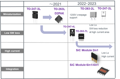
ROHM’s discretes and module packaging span a wide current range to serve application in different parts of the power spectrum from charging stations and onboard chargers (OBCs) to traction inverters and solar inverters (Figure 4).
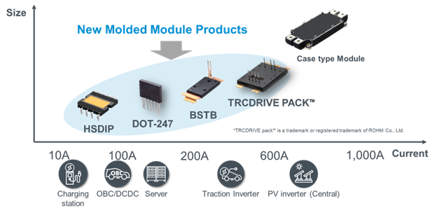
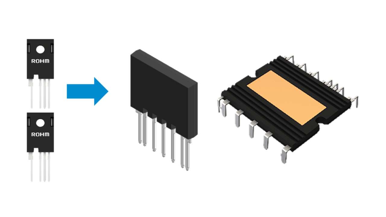
This article focuses on the HSDIP and DOT-247 form factors (Figure 5). The HSDIP power modules integrate 4 or 6 SiC MOSFETs in a single, small package. The diverse lineup of on-resistance options covers application needs for 7kW-22kW EV OBCs and other applications in a similar power range, improving power density compared to discrete-based conventional designs.
The DOT-247 module takes form similar to through-hole type packaging and is approximately twice as large as the conventional TO-247 package. This allows for the integration of two SiC MOSFETs in the package while offering very low conduction loss (or low Ron) compared to TO-247 options.
A Look at the HSDIP Package
What Is the HSDIP Package?
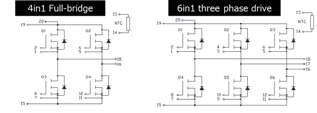
ROHM’s HSDIP module leverages 750-V and 1200-V Gen 4 SiC MOSFETs to integrate full-bridge topology (4-in-1), three-phase drive (6-in-1), or hybrid topology (2-in-1 and 4-in-1) in the same 31 x 38 x 8.5 mm (WxLxH) package size (See Figure 6 and Table 1).
The HSDIP offers several inherent advantages including:
- Simplified isolation design by removing the need for an isolation sheet
- Miniaturization via high integration
- High frequency operation with driver source terminals
| Topology | Potential application circuit | Vdss | Ron |
| 4-in-1
|
7~11kW full‐bridge LLC resonant converter | 750-V | 13 mΩ |
| 26 mΩ | |||
| 45 mΩ | |||
| 7~22kW full‐bridge LLC resonant converter | 1200-V | 18 mΩ | |
| 36 mΩ | |||
| 62 mΩ | |||
| 6-in-1 | 7~11kW three-phase PFC | 750-V | 13 mΩ |
| 26 mΩ | |||
| 45 mΩ | |||
| 7~22kW three-phase PFC | 1200-V | 18 mΩ | |
| 36 mΩ | |||
| 62 mΩ | |||
| Hybrid
2-in-1 and 4-in-1 |
11kW PFC totem-pole PFC | 1200-V | 18 mΩ (2-in-1) and 36 mΩ (4-in-1) |
Table 1: HSDIP modules lineup offering different topologies with varying Vdss and Ron values depending upon the Gen 4 SiC MOSFET ratings employed.
As shown in Equation 1, the inherently low Ron values of the Gen 4 technology minimize conduction losses to achieve higher power; for up to 22 kW three-phase PFCs found in onboard chargers (OBCs) and 22 kW full-bridge LLC resonant converters.
Conduction loss = I2 x Ron
(Equation 1)
The Benefits of HSDIP Over Other SiC Package Technologies
The HSDIP incorporates an increased creepage distance over traditional package technologies such as TO-247 and conventional DIP. The creepage and clearance distances are isolation distances between the pins of the SiC package where creepage is the shortest distance between adjacent pins over a surface while clearance is the shortest distance between pins through air. Creepage distance will relate to tracking failures, or failures due to the insulating material while minimum clearance distances are maintained to ensure there is no flashover or electrical arcing between pins.
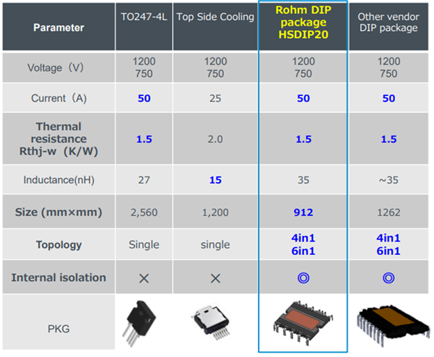
Table 2 compares the HSDIP20 with other SiC packages on the market in terms of voltage, current, Rth, inductance, size, topology, and internal isolation. Furthermore, the HSDIP package is internally isolated to facilitate easier assembly to the heatsink. The advanced isolation of the HSDIP removes the need for additional isolation sheet while maintaining 2500 Vrms isolation voltage from terminal to heat sink. Alternative technologies such as TO247-4L and top side cooling packages do not have this level of built-in internal isolation. Moreover, conventional DIP modules generally do not support multiple topologies with up to 6 SiC FETs integrated (6-in-1). Typically, a 4-in-1 topology is exclusively available at different Ron values. A low stray inductance (Ls) allows for noise-free high frequency drives. It is also important to note that there is over 25% size reduction in HSDIP package when compared to other DIP packages.
Using the HSDIP in OBCs and DC/DC Converters
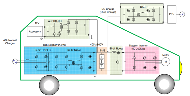
The integration of 4 to 6 SiC FETs in the HSDIP package makes it suitable for many power circuits such as those found in EVs (e.g., OBCs, exciters, e-compressors). An example of EV architecture can be seen in Figure 7 starting from front to back with the motor being driven by a 50 to 200 kW traction inverter (pink block); a bidirectional boost converter (light green block, optional); a BMS, or battery management system, to monitor the voltage, current, and temperature of individual battery cells and perform cell balancing (orange block); and a 3.3 kW to 22 kW bidirectional OBC consisting of a full-bridge CLLC (symmetric LLC) resonant converter and bidirectional totem-pole PFC (blue block) for AC charging. A dual active bridge (DAB) converter can be used for fast DC charging of the battery (green block). While an auxiliary DC/DC converter is used for 12-V vehicle accessories.
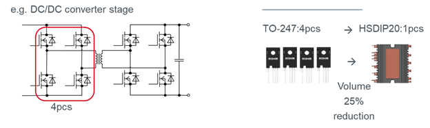
As stated earlier the 4-in-1 configuration supports full-bridge topologies such as LLC resonant converters and DAB ranging from 7kW~22kW, dependent upon the Gen 4 SiC technology employed. As shown in Figure 8, part of the DC/DC converter stage can be realized with a singular HSDIP20 package instead of four separate TO-247 packages, a 25% reduction in volume.
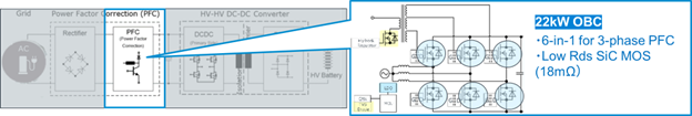
The 6-in-1 configuration can, for instance, ease the design of a three-phase drive commonly found in the OBCs of EVs (Figure 9). This is a capability that is not typical of competitor DIP modules: the Ron values are at least 2x larger, making it difficult to reach higher power capabilities and the 6-in-1 configuration is not often supported by the DIP package.
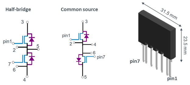
A Look at the DOT-247 Package
What Is the DOT-247-7L Package?
The DOT-247 supports a diverse range of power electronic applications in automotive and industrial markets (Figure 10). In principle, the DOT-247 in either half-bridge or common-source configurations can be deployed in applications that conventionally utilize discrete products such as TO-247s to downsize the system or increase the current handling capability. Applications for the half-bridge topology include boost converters, off-board chargers, uninterruptible power supplies (UPSs), energy storage systems (ESS), and photovoltaic (PV) inverters. The common source configuration is well-suited for matrix converters, neutral point clamped (T-NPC) inverters, as well as battery breakers in EVs and hybrids.
The solution offers the distinct advantages of system miniaturization, increased power handling capacity, optimized thermal and electrical switching performance, and improved power cycling reliability. Furthermore, the DOT-247 maintains compatibility with assembly methods analogous to those employed for conventional through-hole devices.
| Topology | Vdss | Ron | Rated current per arm at 25oC | Automotive or Industrial grade |
| Half-bridge type | 1200 V | 18 mΩ | 76 | Both |
| 1200 V | 9 mΩ | 130 | Both | |
| 1200 V | 11 mΩ | 109 | Industrial | |
| 1200 V | 6 mΩ | 179 | Industrial | |
| 750 V | 13 mΩ | 100 | Both | |
| 750 V | 6.5 mΩ | 165 | Both | |
| 750 V | 8 mΩ | 157 | Industrial | |
| 750 V | 4 mΩ | 230 | Industrial | |
| Common-source type | 1200 V | 18 mΩ | 76 | Both |
| 1200 V | 9 mΩ | 130 | Both | |
| 1200 V | 11 mΩ | 109 | Industrial | |
| 1200 V | 6 mΩ | 179 | Industrial | |
| 750 V | 13 mΩ | 100 | Both | |
| 750 V | 6.5 mΩ | 165 | Both | |
| 750 V | 8 mΩ | 157 | Industrial | |
| 750 V | 4 mΩ | 230 | Industrial |
Table 3: DOT-247 product lineup with 4th Gen. SiC MOSFET.
DOT-247 Versus TO-247
The DOT-247 solution can replace up to six TO-247s with a single package, substantially reducing circuit board space requirement and the parasitic electrical inductances. A comparison between the DOT-247 and a competitor TO-247-4L can be seen in Table 4.
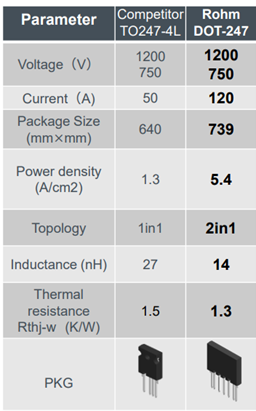
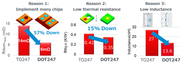
The DOT-247 exceeds the TO-247-4L in virtually every specification, maintaining a much higher power density in a compact package. This is due to the steady improvements found in the 4th generation of ROHM SiC process and packaging technology. The Ron is less than half of that found in the competitor TO-247-4L package (Figure 11), enabling much more power dense circuits. An optimized die-attach configuration with a copper frame design and lead-free solder material offers a much lower thermal resistance from the junction to ambient (Rthj-a) as well as from the junction to the terminal (Rthj-c) which simplifies thermal management. The improved parasitic inductance ensures users can leverage high frequency drives with significantly less loss.
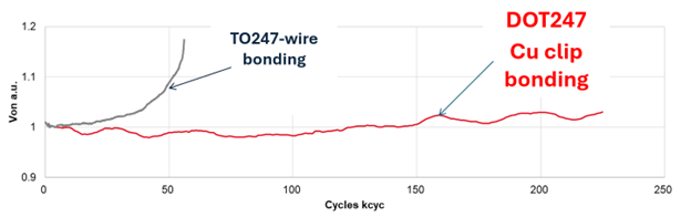
Finally, the copper clip bonding found in the DOT-247 package is much more robust than the wire bonding typically seen in TO-247. This can be seen in the power cycling (PCY) durability tests in Figure 12. Note the DOT-247 has greater than 2x improvements in PCY lifetime compared to wire bonding products.
Using the DOT-247 in Fuel Cell Boost Converters and Solid-State Circuit Breakers
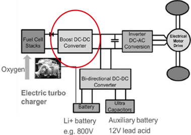
Figure 13 shows a sample hydrogen fuel cell vehicle (FCV) block diagram where the DOT-247 can be used in the boost converter to replace solutions that utilize either multiple TO-247 discrete or large SiC modules/packs on the market. Much of the available solutions are bulky and costly, limiting the performance of SiC technology with inherently more parasitic. The DOT-247 offers a better solution than the discrete packaging options and the modules/packs, allowing designers to achieve from 15 to 30 kW of power with the FCV boost converter at a 50 kHz switching frequency using the 750-V or 1200-V SiC FETs at ~100 A current levels.
The DOT-247 can also be employed in the common-source configuration for trending solid-state breaker installations that are fast-replacing conventional breakers to enable smart power control. These applications leverage two FETs connected back-to-back. Some key requirements for these power switching devices are to have low conduction losses, generate minimal heat, and be in a compact package. The DOT-247 in a common-source topology provides a much lower Ron than standard discrete products, minimizing losses and optimizing efficiency—a factor that will in turn, reduce space requirements and minimize heat generation.
Conclusion
To meet the demand for more compact and energy efficient design in EV and industrial power converter systems, ROHM developed two innovative module packages that allow designers to take advantage of the exceptional characteristics of SiC power devices in small form factors with wide ranges of target power levels, and a high degree of reliability. This begins by leveraging ROHM’s 4th gen SiC MOSFET with industry-leading low specific on-resistance. The HSDIP and DOT-247 power modules are available at 750-V and 1200-V voltage ratings and offer very distinct advantages compared to alternative solutions with comparable power handling capabilities.
References
- Luhong Xie, Erping Deng, Shaohua Yang, Ying Zhang, Yan Zhong, Yanhao Wang, Yongzhang Huang, State-of-the-art of the bond wire failure mechanism and power cycling lifetime in power electronics, Microelectronics Reliability, Volume 147, 2023.