The age-old parable of the tortoise and the hare seems to have implications in the world of signal processing. Certain signal processing tasks, such as precisely selecting frequency channels, require slower data transfer rates. Optical waves that move at the speed of light simply move too fast when data needs to be delayed over time scales of tens of nano-seconds.
The problem is not new; analog electronic circuits have been facing similar challenges in signal processing for 60 years. Engineers solved the problem by converting signals from the electrical domain to acoustic waves. The speed of sound, of course, is slower than that of light by a factor of 100,000. Acoustic waves acquire the necessary delays over tens of micro-meters instead of meters. Such path lengths are easily accommodated on-chip. Following propagation, the delayed signal can be converted back to electronics.
A team led by Prof. Avi Zadok of Bar-Ilan University’s Faculty of Engineering and Institute of Nanotechnology and Advanced Materials translated this principle to silicon-photonic circuits.
“There are several difficulties with introducing acoustic waves to silicon chips,” says doctoral student Dvir Munk, of Bar-Ilan University, who participated in the study. “The standard layer structure used for silicon photonics is called silicon on insulator. While this structure guides light very effectively, it cannot confine and guide sound waves. Instead, acoustic waves just leak away.”
Due to this difficulty, previous works that combine light and sound waves in silicon do not involve the standard layer structure. Alternatively, hybrid integration of additional, nonstandard materials was necessary.
By creating acoustic waves that propagate at the upper surface of the silicon chip, the waves don’t leak down as quickly.
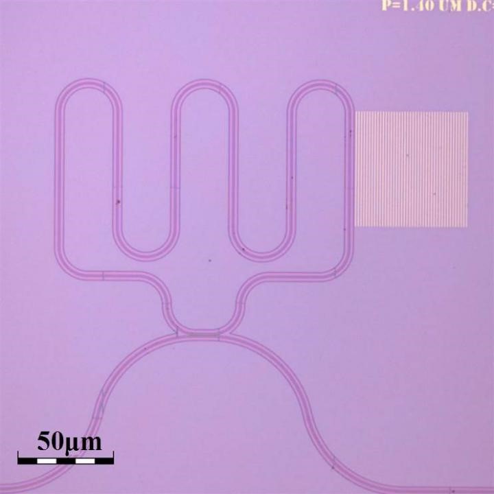
The researchers also sought to avoid using piezo-electric crystals, typically used to generate acoustic waves. Instead, the researchers illuminated metals to carry the signal of interest. The metals expand and contract, straining the silicon surface below to drive surface acoustic waves. The waves pass across standard optical waveguides in the same chip, and the light in those waveguides is affected by the surface waves, converting the signal of interest from one optical wave to another via acoustics. The result: Significant delay across a small area.
The concept combines light and sound in standard silicon with no suspension of membranes or the use of piezo-electric crystals. Acoustic frequencies up to 8 GHz are reached, however, the concept is scalable to 100 GHz. The working principle is applicable to any substrate, not only silicon.
Researchers see potential applications for the technology in future 5G cellular networks.