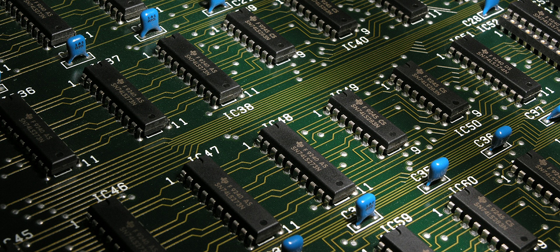
An ESOMAR-certified market research company recently published semiconductor wafers market study which projects a largely positive growth trajectory for the 2020-2030 assessment period. The study divulges key dynamics responsible for shaping the future growth prospects of the market.
Deepening 5G technology penetration is amongst the primary growth drivers, as business houses and corporates look towards diversifying their future operations. By 2024, 5G networks shall cover 2/5th of the globe, handing a quarter of all mobile traffic data. Thus, production of wafers to manufacture ICs for 5G devices is rising.
Manufacturers are increasingly preferring gallium nitride semiconductor chips over the conventional silicon based chips, as the latter tends to have less temperature tolerance.
Key Takeaways
- By application, automotive semiconductor wafer to experience nearly twofold growth until 2030.
- Extensive applications to be witnessed across consumer electronics, particularly in the manufacturing of integrated circuits (ICs).
- By size, 150-200 mm semiconductor wafers is likely to generate over 2/3rd revenue share by 2020-end.
- East Asia to emerge as the market hegemon, with China pivoting maximum growth, Europe and North America remain highly lucrative.
- Global semiconductor wafers market to register value CAGR worth 5.6% through 2030.
“Growing penetration of automation is accelerating demand for self-driven vehicles, an application area which is anticipated to generate lucrative growth prospects for leading semiconductor wafer manufacturers,” remarked the report analyst.
COVID-19 Impact Analysis
The novel coronavirus pandemic has ushered in multiple impacts across the global semiconductor wafers market. Stringent government-mandated lockdowns have contracted production of automotive,s a key application area for semiconductor wafers.
A 16% decline was experienced in the global automotive industry since the past few months, thereby restraining sales of semiconductor wafers for multiple purposes such as infotainment systems, collision detection and navigation.
Simultaneously, surging sales of consumer electronic products is keeping the semiconductor wafers market demand afloat, particularly across emerging economies. With mandatory lockdowns imposed, corporate entities, educational institutions and entertainment houses are encouraging virtual interactions, thus upscaling demand for smartphones, tablets and laptops.
Taking the aforementioned trends into account, the semiconductor wafers market is likely to experience a moderate dip in the short-run, after which growth is expected to rebound on the back of easing restrictions.
Competitive Landscape
Prominent semiconductor wafers manufacturers profiled in the report include Applied Materials, ASM International, Nikon, SCREEN Semiconductor Solutions, Hitachi High-Technologies, Tokyo Electron, ASML, KLA, Lam Research and others.
In November 2020, Hitachi High-Technologies Corporation launched its 3D SEM CT1000 used for defect observation across semiconductors. The devices enable a three-dimensional observation of pattern and defects shapes occurring during the manufacturing process on wafers measuring upto 200 mm in diameter.
In December 2020, Tokyo Electron Limited (TEL) announced the launch of its CELLESTATM SCD single wafer cleaning system, scheduled to hit the shelves by January 2021. The product is a collapse-free drying method which uses a supercritical fluid and is expected to ease semiconductor wafer cleaning processes.