Resonant-tunneling diodes (RTDs) are used in high-frequency oscillators, wave emitters and detectors, logic gates, photodetectors, and optoelectronic circuits. Marcio Daldin Teodoro, a professor in the Physics Department of the Federal University of São Carlos (UFSCar), in the state of São Paulo, Brazil, was the principal investigator for a study that determined charge buildup and dynamics in RTDs throughout the applied voltage range.
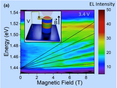
RTD-based devices operation depends on several parameters including charge excitation, accumulation and transport, and the relationships among these properties. Charge carrier density in these devices is determined before and after the resonance area, but not in the resonance area itself, which carries the key information. In the research, the team used advanced spectroscopy and electronic transport techniques to determine charge accumulation and dynamics throughout the device. The tunneling signature is a peak current followed by a sharp drop to a specific voltage that depends on the RTD’s structural characteristics.
Diodes are widely used electronic devices that act as one-way switches for current. There is a special class of diodes designed to make use of the phenomenon known as “quantum tunneling”. RTDs are among the fastest semiconductor devices and have countless practical applications, such as high-frequency oscillators in the terahertz band, wave emitters, wave detectors, and logic gates. They are also sensitive to light and can be used as photodetectors or optically active elements in optoelectronic circuits.
Quantum tunneling is where particles are able to transition through a classically forbidden energy state. They escape from a region surrounded by a potential barrier even if their kinetic energy is lower than the potential energy of the barrier. The RTDs consist of two potential barriers separated by a layer that forms a quantum well. The structure is sandwiched between extremities formed by semiconductor alloys with a high concentration of electrical charges and accelerated when a voltage is placed across the RTD. The tunnel effect occurs when the energy in the electrical charges accelerated by application of the voltage coincides with the quantized energy level in the quantum well.
As the voltage is applied, the energy of the electrons retained by the barrier increases, and at a specific level, they are able to cross the forbidden region. However, if an even higher voltage is applied, the electrons can no longer get through because their energy exceeds the quantized energy in the well, explained Marcio Daldin Teodoro.
The study can guide further research on RTDs, leading to the production of more efficient optoelectronic devices. By monitoring charge buildup as a function of voltage, it will be possible to develop novel RTDs with optimized charge distribution to enhance photodetection efficiency or minimize optical losses.
The paper “Determination of carrier density and dynamics via magneto-electroluminescence spectroscopy in resonant-tunneling diodes” is at: journals.aps.org/prapplied/abstract/10.1103/PhysRevApplied.15.014042.
Original Source: Eureka Alert