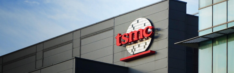
At its 2025 North America Technology Symposium, Taiwan Semiconductor Manufacturing Company (TSMC) unveiled its most advanced logic process yet: A14. Slated for production in 2028, the new node is designed to meet the rising demands of AI, smartphones, automotive, and IoT markets—offering up to 15% better performance or 30% lower power consumption than its predecessor, N2, and boosting logic density by more than 20%.
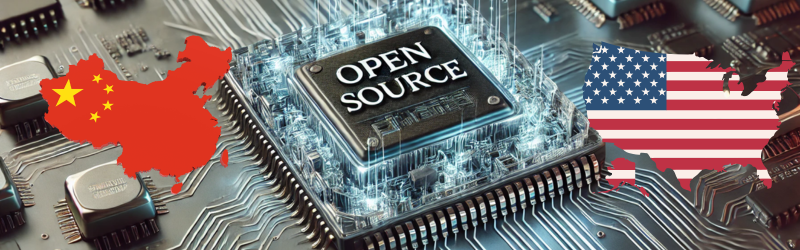
This announcement comes at a pivotal moment for the semiconductor industry, as geopolitical tensions and a renewed focus on semiconductor self-sufficiency continue to shape supply chains. The U.S. recently expanded tariffs on certain Chinese-made tech components, including legacy semiconductors, prompting American companies to deepen partnerships with non-Chinese foundries like TSMC. In fact, the U.S. government’s CHIPS and Science Act funding has helped accelerate stateside semiconductor investment, with TSMC currently building fabs in Arizona aimed at 3nm production.
Why A14 Matters
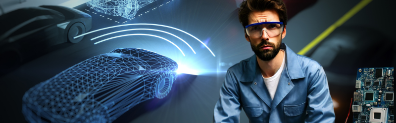
TSMC’s A14 process is more than just a technical milestone—it’s a key enabler for next-generation AI systems and edge computing. With AI models rapidly scaling in size and complexity, the need for chips that can compute faster and more efficiently has never been more urgent. A14’s promise of higher speed and lower power makes it ideal for the data-hungry demands of generative AI, large language models, and real-time inference engines, all of which are moving from the cloud to the edge.
As devices from smartphones to vehicles incorporate more AI at the edge, A14’s role becomes clearer. The process supports TSMC’s NanoFlex™ Pro standard cell architecture, allowing designers to optimize for either power or performance based on application—whether it’s a smart camera, an in-vehicle assistant, or a battery-powered IoT sensor.
The Bigger Picture: Chips as Infrastructure
At the same time TSMC pushes the boundary of what’s possible at the nanoscale, governments are rethinking semiconductors as critical infrastructure. The recently proposed American Semiconductor Resilience Act would extend funding for domestic chipmaking beyond initial CHIPS Act investments, signaling a long-term shift in how governments treat semiconductor security.
TSMC’s A14 process, developed in Taiwan but destined to support global supply chains—including possible U.S. fabs—represents the balancing act chipmakers must maintain: staying ahead of technology curves while navigating trade restrictions and national security concerns.
Expanding the Ecosystem
Beyond the A14 announcement, TSMC also unveiled key innovations in packaging and integration. Its CoWoS® packaging will scale up to 9.5 reticle sizes by 2027, supporting as many as 12 HBM (High Bandwidth Memory) stacks per package—a major leap for AI and high-performance computing systems.
Meanwhile, its System-on-Wafer (SoW-X) platform takes chip integration to a radical level, delivering computing power 40x greater than conventional CoWoS systems, with volume production also expected in 2027. These developments directly address bottlenecks in AI system performance and cost.
Other notable updates include:
-
Smartphone Tech: N4C RF process shrinks area and power needs for next-gen 5G and Wi-Fi 8 devices.
-
Automotive Focus: The N3A process meets strict automotive standards, targeting the high-reliability needs of ADAS and autonomous driving.
-
IoT Advancements: N6e and upcoming N4e processes reduce power draw in edge-AI devices like smart home sensors and wearables.
A Glimpse Into the Innovation Zone
This year’s North America symposium also spotlighted emerging companies in its “Innovation Zone,” where startup participants showcased their ideas to investors and peers. As semiconductors continue to be the foundation of emerging tech—from quantum computing to neuromorphic chips—events like this serve as springboards for the next generation of innovation.
Final Thoughts
With the A14 process, TSMC reinforces its role not just as a contract manufacturer, but as a bellwether for where global computing is headed. As AI adoption accelerates and trade winds shift, the importance of accessible, efficient, and geopolitically resilient semiconductor technology has never been clearer.
In a world where everything is becoming a computing device, TSMC’s A14 is a glimpse into the chips that will make it possible—and the complex landscape required to build them.