


At this week’s Imec Technology Forum (ITF 2018) in Antwerp, imec and Unisantis announced significant progress in the joint development of a process flow targeting an SGT 6T-SRAM cell with areas between 0.0184 and 0.0205 square micrometer, meeting or exceeding the dense cell area in a N5 technology node.
Studies show that the vertical gate-all-around SGT-based cells have a 20-30% reduced area compared to horizontal gate-all-around FETs, while also outperforming these in terms of operating voltage, standby leakage and stability.
The Surrounding Gate Transistor is a vertical gate-all-around architecture that was developed at Unisantis as the basis for a universal silicon technology platform for DRAM, NAND, Flash, and SRAM.
“SGTs have all the advantages of horizontal gate-all-around transistors, allowing a near-perfect electrostatic control of the transistor channel,” said Professor Fujio Masuoka, Director and CTO at Unisantis and inventor of the SGT concept. “But because the channel is a vertical pillar, the concept has the potential for a significant area reduction compared to horizontal nanowire-based transistors.”
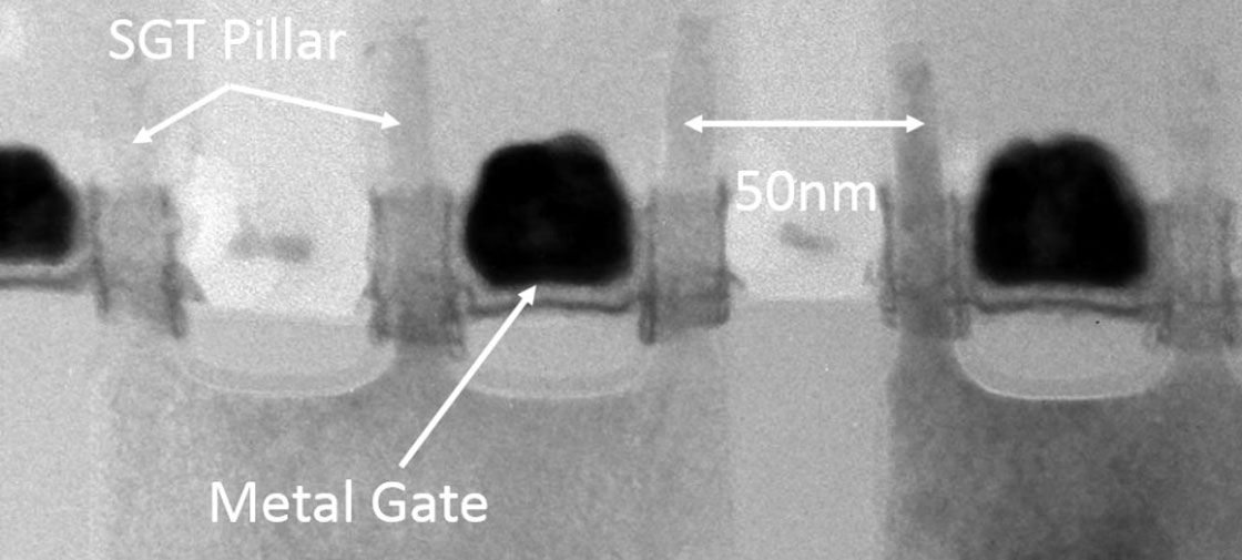
Imec and Unisantis worked out the key process flow and steps for a 6T-SRAM cell using SGT. Through a novel Design process Technology Co-Optimization (DTCO), the researchers were able to develop an SRAM bit-cell area of 0.0205 square micrometer, using a minimum pillar pitch of 50nm. This is a 24% improved scaling factor compared to the smallest SRAM designs published to date, and makes the design ready for an N5 technology node. A key technical challenge that was solved involved the mechanical stability of the pillars at the high aspect ratios that were required. Through the use of single-exposure EUV lithography, the number of process steps could be reduced, resulting in an estimated cost comparable to that of FinFET-based SRAM.
“We’re excited to present the results of this joint project,” said Dan Mocuta, the Logic Device and Integration department director at imec.
“In a concerted effort and using the tools and expertise available in house, the imec and Unisantis engineers were able to design and are well on their way to fabricating these record-scaled SRAM cells. This again proves the value of our expertise for R&D collaborations, as well as the leading-edge abilities of our cleanroom platform.”