
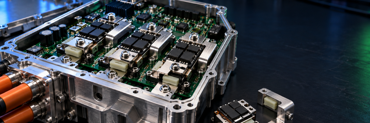

An experimental 400 V, 2.5 kW variable-speed drive replaces soldered interconnects with clamped contacts. The result is a serious attempt to make repair part of power-electronics design rather than an afterthought.
A failed power transistor often turns a serviceable inverter into scrap.
That outcome is rarely caused by a lack of intelligence in the control software or a shortage of replacement semiconductors. It starts with the physical assembly. Power devices are soldered to boards and bus structures, pressed into packages that were never meant to reopen, then expected to survive years of electrical, thermal and mechanical stress. When one component fails, repair often means heating, desoldering, cleaning pads and hoping the reworked assembly will still meet its original electrical and thermal requirements. In many cases, replacement of the entire module is simpler.
A research team at ETH Zurich has taken a different route. Their three-phase variable-speed drive uses no soldered electrical interconnects in its power stage. Instead, the 400 V, 2.5 kW GaN inverter relies on screw-clamped resin molds and rubber compression pads to hold the electrical contacts together. The point is not novelty for its own sake. The authors are asking whether a kilowatt-class converter could be built for disassembly and repair without giving up the low-resistance connections and ruggedness that power electronics demand.
Their answer, at least in an early prototype, is encouraging. The inverter completed 120 thermal cycles with heatsink temperatures up to 90°C without a measured increase in effective on-state resistance. It also remained electrically intact through powered vibration sweeps from 5 Hz to 2 kHz at acceleration levels above 10 g. After a deliberate transistor failure, the team replaced the device without destroying the assembly, then demonstrated component reuse.
It is a small inverter by traction-drive standards and a large one by board-level electronics standards. More important, it exposes a design tension that has become easy to ignore: modularity is not the same thing as repairability.
A module is not necessarily repairable
Power electronics already has plenty of modular products. Engineers specify half-bridges, intelligent power modules, power stages and packaged drives precisely because integration reduces development time and simplifies assembly. But modularity usually stops at the outside of the enclosure. A module is replaceable as a unit, while the components inside remain permanently joined.
That arrangement works well for manufacturing. Solder delivers an electrically conductive joint at high production volumes and established assembly processes support it. It also locks together parts made from materials with different coefficients of thermal expansion. As the assembly heats and cools, solder joints absorb some of the resulting strain. The reliability literature has long treated thermal fatigue in solder joints as a central packaging problem, especially where repeated temperature change and material mismatch drive damage at the microstructural level.
For a repair-oriented inverter, the challenge changes. The electrical connection must remain stable without solder, even as the structure expands, vibrates and carries high-frequency switching current. It also needs to reopen without damaging the transistor, PCB or contact surfaces.
That is a much harder job than adding a removable cover.
The ETH Zurich design uses 650 V gallium-nitride transistors and switches at 200 kHz. GaN makes the question more demanding. Fast switching improves power density and enables smaller passive components, but it also raises the importance of the physical current path. A connection that seems acceptable at low frequency can introduce unwanted inductance, resistance or inconsistency when used in a fast power stage.
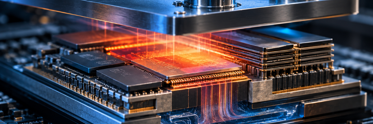
The researchers therefore did not build a large, loose mechanical assembly and call it repairable. They developed a clamping arrangement around the same PCB used in a soldered reference inverter. Resin molds, tightened with screws, apply pressure through rubber pads that maintain contact between the board and the power components. The molds create a controlled mechanical structure while the pads help distribute force over the contact areas.
The approach treats contact pressure as a core electrical design parameter. That is the crucial shift.
The contact is now part of the power stage
Solder joints disappear into a layout drawing. Their geometry matters, but once the manufacturing process is qualified, they are often treated as fixed infrastructure. A clamped contact is more visible. Its performance depends on pressure, surface finish, alignment, compliance, temperature and the repeatability of the assembly process.
That sounds like a drawback, and it is one. A solderless converter has more variables to control.
Yet it also makes the tradeoffs explicit. The mechanical design no longer sits downstream of the electrical design. It becomes part of the current path.
The paper’s tests focus on whether that current path stayed intact. In thermal cycling, the researchers brought the heatsink temperature to 90°C for 120 cycles and monitored the effective on-state resistance, including contact resistance. They report no degradation in that value. That result matters because rising contact resistance is one of the first places a pressure-contact scheme would reveal trouble. Higher resistance means higher loss, more heat and potentially more relaxation of the mechanical structure. The experiment did not show that progression. [1]
The vibration result is equally important. The group ran an open-loop sweep between 5 Hz and 2 kHz with acceleration amplitudes beyond 10 g while the inverter remained energized. The demonstrator stayed electrically functional throughout the test. Follow-up resistance measurements and nominal-power operation also found no contact degradation.
Those results do not establish a lifetime rating. They do establish something more basic and useful: a solderless architecture does not automatically fall apart when exposed to the sorts of thermal and mechanical stresses that power-converter designers worry about.
That distinction is worth preserving. A prototype that survives 120 cycles is not a substitute for a long-term qualification campaign. It does not answer every question about humidity, corrosion, dust ingress, shock, field assembly variation or years of clamp-force relaxation. The paper is a demonstration of feasibility, not a finished commercial platform. Still, the work clears an important threshold. The concept has moved beyond an elegant CAD model.
Repair after failure, not replacement before failure
The most compelling part of the work is not the thermal plot or vibration trace. It is the failed transistor.
The researchers intentionally replaced a failed power device by opening the clamped structure, removing the damaged part and reassembling the inverter with another transistor. The process avoided destructive teardown. They also reused components, which is the practical test of whether a repairable architecture is truly repairable.
That changes the service model.
In a conventional soldered power stage, repair decisions usually happen at the module level. A technician replaces an assembly because diagnosing and reworking individual devices is too labor-intensive, too risky or both. In a solderless design, service potentially moves down a level. The failed device becomes accessible, and the remaining hardware retains value.
There are limits. Access to a transistor does not make field repair easy. A service procedure still needs torque specifications, inspection criteria, ESD controls, component traceability and a way to confirm that the rebuilt power stage meets its insulation, thermal and switching requirements. Repairability creates more process responsibility, not less.
But that responsibility is manageable when it is designed in from the beginning.
It also creates choices for manufacturers. A company could use a clamped design for depot-level repair rather than field repair. It could reserve component replacement for high-value industrial drives where downtime and replacement cost justify the service process. It could build the same mechanical architecture into a family of products and decide which models expose repair access.
The important point is that the decision remains available. Soldered construction often removes it before the product leaves the factory.
The environmental case is not automatic
Repairability is frequently framed as an environmental virtue, but the paper does not take that shortcut.
The initial life-cycle assessment found that the solderless demonstrator had a higher embodied carbon footprint than the soldered reference. The reason was not mysterious. The experimental design used 3D-printed resin molds, and those molds carry an environmental cost. When the authors evaluated an injection-molding scenario instead, the carbon footprint moved close to that of the soldered reference.
That finding deserves more attention than it will probably receive.
A repairable product is not automatically lower impact if its new mechanical hardware adds substantial material, processing or transport burdens. The environmental outcome depends on the manufacturing method, the production volume, the number of repairs achieved and the service life gained. A one-off prototype optimized for laboratory flexibility is not the same thing as a production inverter optimized for material efficiency.
For engineers, this is a useful reminder that circular design requires an accounting exercise. The right question is not whether a product has replaceable parts. It is whether the extra material and manufacturing complexity are repaid through longer use, recovered components and avoided replacement assemblies.
The researchers’ injection-molding comparison suggests that the answer could be yes, provided the mechanical interface is designed for scalable manufacture. That is a different claim from saying every converter should abandon solder tomorrow.
Where this idea fits
The demonstrated inverter is a 400 V DC, 2.5 kW, three-phase variable-speed drive. That places it in a familiar part of the power-electronics landscape: industrial motor control, mobile machinery, compact drives and other systems where high switching frequency and serviceability meet. The voltage also sits close to the lower edge of architectures familiar to electric-vehicle engineers, though this paper is not an automotive traction-inverter qualification study.
The idea travels further than the exact power rating.
Data-center power shelves, robotics, renewable-energy converters, automated manufacturing equipment and distributed energy systems all face a version of the same question. When a semiconductor fails, should the rest of the hardware become waste? In high-value equipment, the answer increasingly ought to be no.
A solderless contact scheme will not suit every application. High-volume products with short service lives might not justify the added structure. Environments with severe contamination could demand more elaborate sealing. Some products need the lowest possible cost more than repair access. Others require qualification evidence far beyond what this paper presents.
Still, the experiment gives design teams a better starting point than a philosophical argument about circularity. It offers a functional inverter, a soldered reference, thermal testing, vibration testing, a repair demonstration and a preliminary life-cycle comparison.
That is enough to change the conversation.
The lesson is not that solder is obsolete. Solder remains one of the most capable joining technologies in electronics. The lesson is that it has quietly dictated the end-of-life behavior of many power systems. When designers want a converter to come apart, they need to design the electrical joint, the mechanical load path and the service procedure together.
This GaN inverter does exactly that. It turns the contact interface into an engineered subsystem rather than a permanent manufacturing detail. For repairable power electronics, that is where the real work begins.
Sources
[1] Luc Imperiali, Aaron Griesser and Jonas Huber, “Modularity is Not Enough: Demonstration of a Solderless 400 V DC, 2.5 kW Three-Phase Inverter,” September 23, 2026. arxiv.org
[2] J. W. Xian et al., “The Role of Microstructure in the Thermal Fatigue of Solder Joints,” Microelectronics Reliability, 2023.