
AI accelerators are generating more heat inside increasingly complex packages. New research shows why keeping them cool requires more than an effective cold plate.
A liquid-cooled server could have an excellent cooling system and still struggle to keep its processor within operating temperature limits. The problem begins long before the heat reaches the coolant.
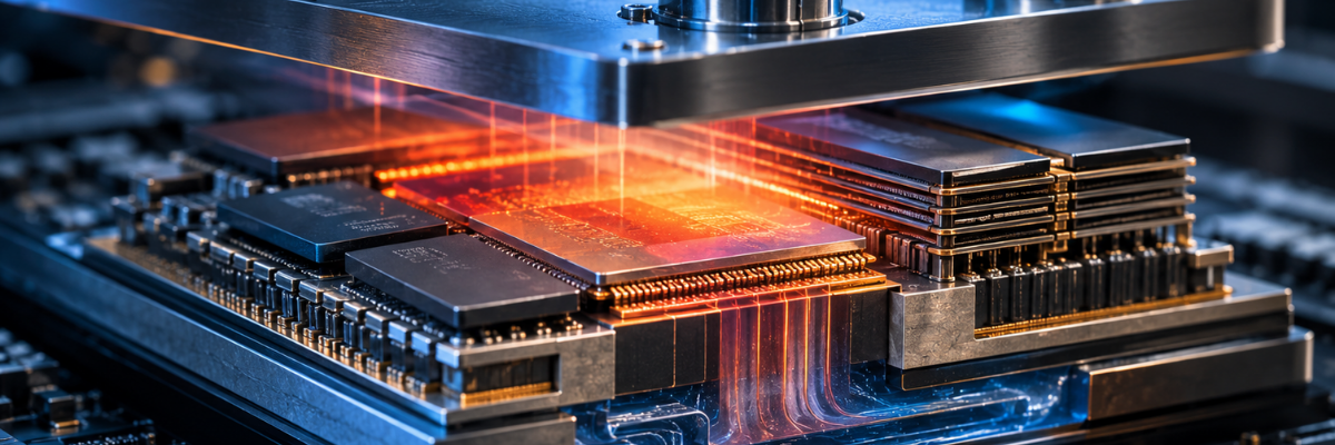
Inside an advanced AI accelerator, heat travels through silicon, bonding materials, thermal interfaces and other packaging structures before reaching a heat spreader or cold plate. Every layer adds thermal resistance. Meanwhile, computing dies and stacks of high-bandwidth memory (HBM) generate heat in different locations, often within the same package.
Bringing these components closer together improves data transfer, but it also complicates the path heat must take to escape.
A review published September 8 in Micromachines examines how increasingly tall HBM stacks and finer interconnects contribute to heat accumulation, localized hotspots and mechanical reliability problems. The researchers argue that thermal performance, material interfaces and mechanical stress need to be considered together rather than addressed as separate design problems.
The issue is also shaping commercial packaging development. In May, SK hynix introduced an HBM architecture that incorporates additional cooling elements directly into the memory package. The company reports a 30% reduction in thermal resistance compared with its reference design.
Both developments point to the same engineering challenge: removing heat from the server is only part of the job. Engineers must first get it out of the semiconductor package.
More Computing Power, More Complicated Heat Paths
Today’s AI accelerators illustrate the scale of the problem. AMD’s Instinct MI350 series combines eight GPU chiplets with 288GB of HBM3E and up to 8TB/s of memory bandwidth. The MI355X has a typical board power rating of 1,400W, according to AMD’s specifications. That figure covers the accelerator module rather than an individual silicon die, but it demonstrates the amount of heat that system designers must accommodate.
The packaging architecture is as important as the power figure.
Instead of placing every function on a single large die, advanced processors increasingly distribute computing and memory functions across multiple pieces of silicon. Chiplets allow designers to combine specialized dies in one package, often using dense interconnects that move data over much shorter distances than conventional board-level connections.
That arrangement changes how heat moves.
Different dies produce different amounts of heat. Some operate near particularly active regions of neighboring components. Others sit farther from the cooling surface or beneath additional layers of silicon.
Consequently, the hottest part of a package isn’t necessarily the component consuming the most total power. Its location and available heat-transfer path also matter.
A chiplet surrounded by other active components might have fewer effective paths for dissipating heat than an identical die placed elsewhere in the package.
For packaging engineers, this makes the physical arrangement of the silicon a thermal-design decision as well as an electrical one.
The Cold Plate Is Only the Last Stop
Consider what happens inside a liquid-cooled accelerator.
Heat generated by the transistors travels through the silicon and package materials. It passes through thermal interfaces and a heat spreader before reaching the cold plate, where circulating liquid carries it away.
The cold plate might be highly effective at removing heat from its own surface. It cannot eliminate the resistance encountered between that surface and the transistors.
A simplified relationship illustrates the problem:
Here, ΔT is the temperature difference across a thermal path, Q is the rate of heat transfer and Rth is the thermal resistance.
If the amount of heat increases without a corresponding reduction in thermal resistance, the temperature difference rises.
Real semiconductor packages are more complicated because heat spreads in three dimensions. Materials have different thermal conductivities, components generate heat unevenly and interfaces affect how readily heat crosses from one material into another.
Nevertheless, the relationship explains why improving coolant flow alone has limitations.
Heat must reach the coolant first.
Thermal interface materials (TIMs) play an important role in that journey. Even apparently smooth surfaces contain microscopic irregularities. When two solid surfaces meet, tiny gaps reduce effective thermal contact.
A TIM fills those gaps and improves heat transfer.
But thermal conductivity is only one consideration. Engineers must also account for interface thickness, surface flatness, contact pressure and how the material behaves during repeated temperature changes.
The September Micromachines review identifies interfacial thermal resistance as an important contributor to HBM heat accumulation. It also describes how voids, delamination and other interface defects affect both thermal performance and reliability.
An interface that begins to separate under mechanical stress could become less effective at transferring heat. The resulting temperature increase might then contribute to further degradation.
Cooling and reliability are closely connected.
HBM Turns Cooling Into a Three-Dimensional Problem
High-bandwidth memory helps AI accelerators move large amounts of data between memory and processing units without relying on conventional, longer-distance memory connections.
It achieves this performance partly through vertical integration.
HBM stacks multiple DRAM dies and connects them using dense vertical interconnects, including through-silicon vias (TSVs). The arrangement provides substantial memory bandwidth within a compact footprint.
It also creates a difficult thermal environment.
A die buried inside a stack has a different path to the cooling surface than one positioned near the top. Its heat must pass through additional silicon layers, bonding interfaces and other materials.
The Micromachines researchers explain that increasing stack height adds thermal interfaces and complicates heat removal. The temperature distribution depends on the arrangement of the dies, the materials used between them and the available cooling paths.
Heat creates mechanical problems, too.
Silicon, copper, underfill and molding compounds expand by different amounts as their temperatures change. This mismatch generates stress within the package.
Over repeated thermal cycles, stress contributes to risks such as warpage, interfacial delamination and interconnect degradation.
The review also identifies copper protrusion, void formation and joint degradation among the reliability concerns associated with advanced HBM structures.
These effects make material selection more complicated.
An engineer might choose a material for its high thermal conductivity, only to discover that its stiffness creates additional stress or that its processing characteristics make it difficult to form a reliable interface.
The researchers emphasize that improving one material property does not necessarily improve the complete package.
Thermal resistance, adhesion, mechanical stress, electrical behavior and manufacturing requirements must be considered together.
SK hynix Adds a Cooling Path Inside the Memory Package
One commercial development illustrates how manufacturers are responding.
In May 2026, SK hynix introduced iHBM, a packaging approach that places integrated cooling elements within an HBM package.
The company identifies the die-to-die physical-layer region, which connects HBM to the GPU, as a particular area of heat concentration.
Conventional HBM designs rely on indirect heat removal through the core die. SK hynix’s approach introduces an additional path for heat to escape from the concentrated region.
According to the company, the cooling elements use an electrically insulating, thermally conductive silicon-based material. SK hynix reports that the arrangement reduces thermal resistance by 30%.
The distinction is important: this is a manufacturer-reported improvement in thermal resistance, not a claim that the entire AI accelerator operates 30% cooler.
SK hynix says the technology is intended for next-generation HBM products, including HBM5, and is designed for compatibility with existing system-in-package architectures.
The development represents a shift in where cooling occurs.
Rather than relying exclusively on a heat spreader and an external cooling assembly, the manufacturer is modifying the memory package to address heat closer to its source.
Materials Suppliers Are Rethinking the Interface
Other companies are approaching the problem through packaging materials.
At SEMICON Taiwan in September 2026, Dow highlighted silicone technologies designed for advanced semiconductor packaging, including thermal interface materials that transfer heat from the die to the package lid.
The company emphasized the need to consider thermal resistance, bond-line thickness, mechanical stress and long-term reliability together.
According to Dow, increasing power density and heterogeneous integration are making earlier materials evaluation necessary. The company is promoting a development approach in which material properties, package structures and manufacturing conditions are assessed together rather than in isolation.
This matters because a material that transfers heat effectively under laboratory conditions might behave differently inside an operating package.
Temperature cycling, package warpage and differences in material expansion all affect the interface over time.
Dow identifies low bond-line thickness and stable material coverage as important characteristics for transferring heat between a die and its lid.
The trade-offs extend beyond thermal performance.
Increasing the concentration of thermally conductive fillers in a polymer might improve its conductivity but also make the material stiffer or more difficult to process. A more compliant material might accommodate mechanical movement while presenting different thermal limitations.
The September HBM review discusses these competing properties, noting that high filler loading can increase viscosity and elastic modulus, affecting gap filling and stress relaxation.
For engineers, choosing a TIM is therefore not simply a matter of selecting the product with the highest thermal conductivity.
The material must work within the complete package.
Researchers Bring Liquid Cooling Into the Package
Improving the existing heat path is one approach. Another is to shorten it.
Researchers are investigating cooling architectures that move liquid closer to the heat-generating components, reducing the number of interfaces heat must cross.
One example comes from Delft University of Technology. In research published in 2026, the team proposed a direct-to-package cooling approach that embeds microchannels within the package substrate rather than fabricating them directly into the semiconductor.
The design uses small channels to circulate coolant close to the heat source, avoiding some thermal interfaces associated with conventional heatsink arrangements.
The researchers reported heat-flux dissipation of up to approximately 625W/cm² in their experimental system, using around 2–4mL of coolant. They also reported substantially lower junction temperatures and thermal resistance than their air-cooled and conventional heatsink comparison configurations.
Those results apply to the researchers’ specific experimental setup. They do not establish that the architecture is ready for widespread use in commercial AI accelerators.
The approach nevertheless illustrates the attraction of bringing coolant into the package. A shorter thermal path potentially reduces the temperature difference between the heat-generating device and the coolant. It also introduces new design challenges.
Microchannels must distribute liquid evenly while controlling pressure drop. Their small dimensions create concerns involving blockage, manufacturing tolerances and coolant compatibility.
Reliability becomes particularly important when liquid is integrated so closely with expensive semiconductor devices.
Engineers must also consider how to manufacture, inspect and service these structures at scale.
The research shows that cooling architecture is beginning to overlap with semiconductor packaging architecture, rather than remaining a separate system-level decision.
Thermal Design Moves Earlier in Development
These developments change when engineers need to investigate heat.
In a conventional design process, much of the cooling work might occur after the processor and package architecture have been established. Engineers estimate the heat load, select a heatsink or cold plate and design the surrounding cooling system.
That sequence becomes less effective when chiplet placement, die stacking and interface materials determine the internal temperature distribution.
A package might have sufficient overall cooling capacity yet develop a localized hotspot because one die sits behind a particularly resistive thermal path.
Moving that die, changing the stack arrangement or modifying an interface could improve the temperature distribution before any changes are made to the external cooling system.
The September HBM review calls for multiscale thermal-reliability co-design, connecting heat transfer, mechanical stress and electrical behavior across the package and its interconnects.
Dow’s September announcement makes a related point from the materials perspective: packaging materials need to be evaluated earlier, under conditions representative of the final structure and manufacturing process.
These approaches reflect the same underlying problem.
Electrical design determines where heat is generated. Package geometry determines where it travels. Material properties influence both heat transfer and mechanical stress.
A change intended to improve one characteristic could create problems elsewhere.
Thermal analysis therefore needs to inform architectural and materials decisions before the package is finalized.
Cooling Begins Before the Cold Plate
Liquid cooling will remain important as AI accelerators demand more power. Cold plates, coolant distribution systems and rack-level cooling infrastructure all play essential roles.
But advanced packaging introduces thermal problems that external cooling alone cannot resolve.
Heat generated inside an accelerator must pass through an increasingly complicated arrangement of dies, interfaces and structural materials. The position of each component, the properties of each interface and the available paths for heat removal influence the temperature distribution.
Recent HBM research identifies the connection between these thermal pathways and long-term reliability. SK hynix is introducing additional heat-dissipation structures inside memory packages, while materials suppliers and academic researchers are investigating new ways to reduce thermal resistance closer to the silicon.
For engineers, the starting point is changing.
Cooling an AI processor now involves decisions about chiplet placement, memory stacking, interface materials and package construction.
By the time heat reaches the cold plate, many of the most important cooling decisions have already been made.