“The epitaxy growth equipment market for ‘More than Moore’ devices was worth close to $940 million in 2019,” explained Amandine Pizzagalli, Technology & Market Analyst, Semiconductor Manufacturing at Yole Développement (Yole). “And it is expected to reach more than $6bn by 2025 in the aggressive scenario.”
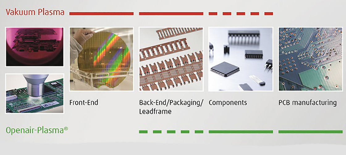
From a technical point of view, MOCVD services the majority of the III-V compound semiconductor epitaxy industry, such as GaAs and GaN based devices. High-Temperature (HT) CVD serves the majority of mainstream silicon-based components and SiC devices.
The new Yole’s technology & market report, ‘Epitaxy Growth Equipment for More Than Moore Devices’ includes the overall silicon and non-silicon based applications. It offers a comprehensive overview of epitaxial semiconductor substrates used in ‘More than Moore’ applications and related equipment.
This analysis presents the technology trends with a wafer market forecast. Yole’s analysts highlight in its new report, the epitaxy growth equipment market trends with detailed forecasts by volume and value. In addition, the competitive landscape and major epitaxy equipment suppliers’ market share are part of this report. The semiconductor industry has been traditionally dominated by silicon substrates.
Although silicon is by far the most dominant today with more than 80% market share, alternative non-silicon-based substrates like GaAs, GaN, SiC and InP are gaining momentum within the ‘More than Moore’ industry. Indeed, new applications emerge along with stringent requirements where silicon solutions are not able to provide expected performances. Consequently, innovative substrate materials have been considered by semiconductor players.
Yole has investigated this industry here, identifying latest innovations and business opportunities.
First, GaN material represents the major epitaxy market after silicon substrates, mostly driven by the traditional LED GaN-devices. However, the overall visible LED industry is currently diversifying its activities to towards more specialized UV and IR LEDs based on GaAs substrates.
Additionally, LED manufacturers are developing new types of LEDs to continue creating value in the consumer displays, such as miniLEDs and microLEDs. Apple is starting this with adoption in its higher-end 2021 smartwatch model. In the best case scenario, microLEDs could also spread into smartphone products, which will definitely reshape the epi-ready wafer market.
On the other hand, WBG materials like SiC substrates have found opportunities in the power electronics market. Here, power consumption reduction is required for electrification of transportation, renewable energy, motor drives and some power supply applications. Despite the high market price of SiC, such substrates are a strong asset for high-voltage applications, and thus are considered as a technology choice for some MOSFET and diode products.
Looking ahead, photonics products laser diodes like VCSELs operating in the IR spectrum and typically processed on GaAs, are making serious inroads into the epitaxy growth market. In addition, GaAs is especially advantageous for RF products such as small-cell implementation, for both sub-6Ghz and the first mmWave small cells in the 28GHz-39GHz range.
Thereby, with the cellphone transition from 4G to 5G, we expect GaAs to remain the mainstream technology for sub-6GHz instead of CMOS . It is the only technology able to meet increasing power level and linearity requirements imposed by antenna board space reductions as well as carrier aggregation and MIMO technology.
Choosing the right substrate technology will strongly depend on the technical performance associated with device requirements, as well as the cost.
“As of today, the epitaxy growth equipment market is mainly driven by LED and power applications,” explained Amandine Pizzagalli from Yole. “In fact, massive subsidies in China have led to an excessive LED capacity build-up. The MOCVD market is now in a situation of significant overcapacity for GaN LED production compared to what is actually produced. MOCVD investment is particularly tough to forecast in the next few years and could change year to year. The situation could be reversed if the government decides to strictly prevent the major LED manufacturers from producing more GaN wafers.”
Therefore, different scenarios have been considered for the traditional LED and microLED markets in the epitaxy growth equipment for More Than Moore Devices report.
For traditional LED GaN-based devices, the MOCVD investment trends will not follow LED wafer demand. Specific upsides and downsides with respect to LED GaN devices might arise as used to happen in the past.
Nevertheless, given recent competitive trends in China, the general lighting and backlighting markets have become commoditized. Hence, epitaxy vendors do not expect significant revenue from these markets going forward. However, requirements for microLED epitaxy in terms of defects and homogeneity are more stringent than traditional LEDs.
There are credible roadmaps for improvement in tools and equipment to reach approximately 0.1 defects/cm2 or less based on defects larger than 1µm. Tighter operating conditions are needed in clean rooms, including for automation and wafer cleaning, compared to traditional LED manufacturing. This is especially true for the smallest dies, below <10µm, which will have smaller killer defects.
Meanwhile, laser diodes represent an additional fast-growing opportunity as the consumer goods industry massively adopts edge-emitting lasers and VCSELs.
By contrast, MEMS industry is small niches of the overall epitaxy growth equipment market, as their production capacity is very well established.
The MOCVD reactor market could be affected by possible technology transitions to MBE for compound semiconductor-based devices like laser diodes, microLEDs and VCSELs.
In fact, MBE could bring greater advantages in terms of yield and uniformity for VCSELs but also for high-frequency 5G RF applications. In the case of SiC power, MOCVD manufacturers are trying to identify and develop new MOCVD technologies to address the SiC market where HT CVD is mostly used.