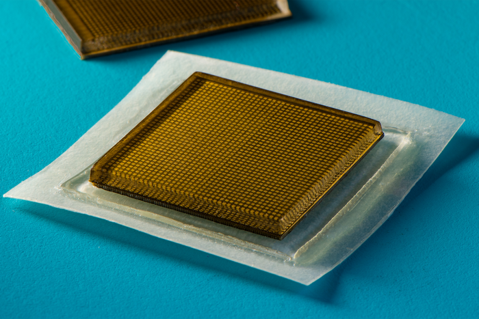
For the first time, researchers showed that a cubic boron arsenide crystal offers high carrier mobility for both electrons and holes – the two ways a charge is carried in a semiconducting material. This is a significant advance for next-generation electronics.
One of two papers published July 22 in the journal Science shows researchers experimentally validated high carrier mobility at room temperature, expanding its potential use in commercial applications. An accompanying paper describes the use of transient reflectivity microscopy to measure the crystal, demonstrating the high mobility and, in some cases, when a higher-energy laser beam was used, exceeding previous predictions.
The work has important implications for a range of electronic and optical applications. Some semiconductor applications require a material with both high thermal conductivity and high electron and hole mobility.
Semiconductors require that current be carried both through electrons and holes, but most known materials offer high mobility only for one type of carrier. The lower value determines the overall efficiency of the semiconductor.
Carrier mobility is measured in the unit of cm2V-1s-1; researchers reported mobility of 1,600 cm2V-1s-1. In the second paper, researchers a range from about 1,500 cm2V-1s-1 to as high as 3,000 cm2V-1s-1.
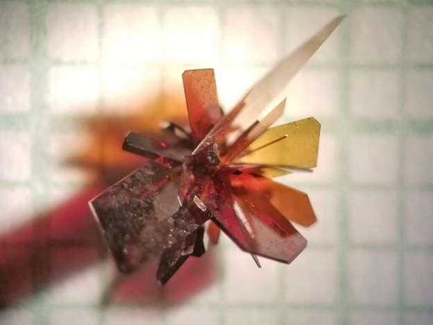
Measuring carrier mobility was complicated because the crystal wasn’t large and uniform, meaning traditional measurement methods such as the Hall effect couldn’t accurately determine its properties. Ionized impurities weakened the material’s performance by strongly scattering the charge carriers, although other impurities – described in the paper as “neutral impurities” – had less impact.
In the second paper, researchers describe the use of transient reflectivity microscopy to measure electron and hole mobility. They used laser pulses to excite carriers in the sample to monitor their diffusion and, in the process, discovered a key difference between the cubic boron arsenide crystal and most semiconducting materials. For example, he said electrons move about four times faster than holes in silicon.
The cubic boron arsenide crystal structure makes it more difficult for the charge carriers to cool, meaning they maintain the heat – and the resulting high mobility – for longer. The researchers reported additional experiments revealed mobility of more than 3,000 cm2V-1s-1, which they attributed to the hot electrons.