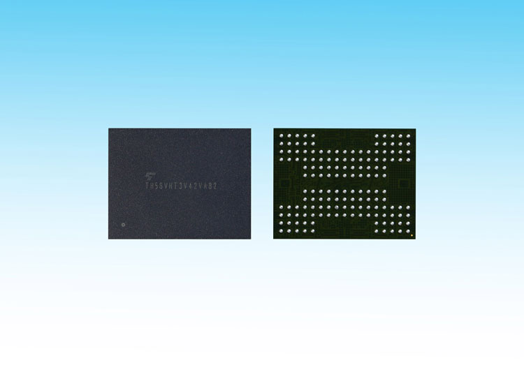
Toshiba Memory has announced development of the world’s first BiCS FLASH 3D flash memory utilizing Through Silicon Via (TSV) technology with 3-bit-per-cell (triple-level cell, TLC) technology. Shipments of prototypes for development purposes started in June, and product samples are scheduled for release in the second half of 2017. The prototype of this ground-breaking device will be showcased at the 2017 Flash Memory Summit in Santa Clara, California, United States, from August 7-10.
Devices fabricated with TSV technology have vertical electrodes and vias that pass through silicon dies to provide connections, an architecture that realizes high speed data input and output while reducing power consumption. Real-world performance has been proven previously, with the introduction of Toshiba’s 2D NAND Flash memory.
Combining a 48-layer 3D flash process and TSV technology has allowed Toshiba Memory Corporation to successfully increase product programming bandwidth while achieving low power consumption. The power efficiency of a single package is approximately twice that of the same generation BiCS FLASH memory fabricated with wire-bonding technology. TSV BiCS FLASH also enables a 1TB device with a 16-die stacked architecture in a single package.
Toshiba Memory Corporation will commercialize BiCS FLASH with TSV technology to provide an ideal solution in respect for storage applications requiring low latency, high bandwidth and high IOPS[7]/Watt, including high-end enterprise SSDs.