Electronics, automation, computers, digital cameras, smartphones, wearables, and even artificial intelligence (AI) would not be possible without silicon semiconductor technology. Advances in semiconductors has reached limits never previously imagined, downscaling the physical size of devices and wires to the nanometer.
Although this technology has been developing since the late 1960s, the miniaturization of circuits seems to have reached a possible halt, since transistors can only be shrunk to a certain size.
Graphene and related two-dimensional (2D) materials offer prospects of unprecedented advances in device performance at the atomic limit, overcoming the limitations of silicon technology.
In a new review article in Nature, a team of international researchers, including researchers at the Institute of Photonic Sciences including Dr. Stijn Goossens and ICREA Prof at ICFO Frank Koppens, plus industrial leaders from IMEC and TSMC, come together to provide an in-depth and thorough review about the opportunities, progress, and challenges of integrating atomically thin materials with Si-based technology.
The team offers insights on how and why 2D materials (2DMs) could overcome current challenges posed by the existing technology and how they can enhance both device component function and performance, boosting the features of future technologies in both computational and non-computational applications.
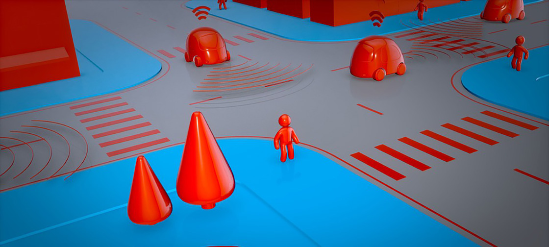
For non-computational applications, the team reviews the possible integration of these materials for cameras, low power optical data communications and gas and bio-sensors. In particular, the team discusses image sensors and photodetectors, where graphene and 2DMs could enable a new vision in the infrared and terahertz range in addition to the visible range of the spectrum. These can serve in autonomous vehicles, security at airports and augmented reality (AR) applications.
For computational systems, in particular in the field of transistors, challenges such as doping, contact resistance and dielectrics/encapsulation can be diminished when integrating 2DMs with Si technology. 2DMs could also radically improve memory and data storage devices with novel switching mechanisms for meta-insulator-metal structures, avoid sneak currents in memory arrays, or even push performance gains of copper wired based circuitry by adhering graphene to the ultrathin copper barrier materials, reducing resistance, scattering and self-heating.
The review offers a roadmap of 2D integration and CMOS technology.