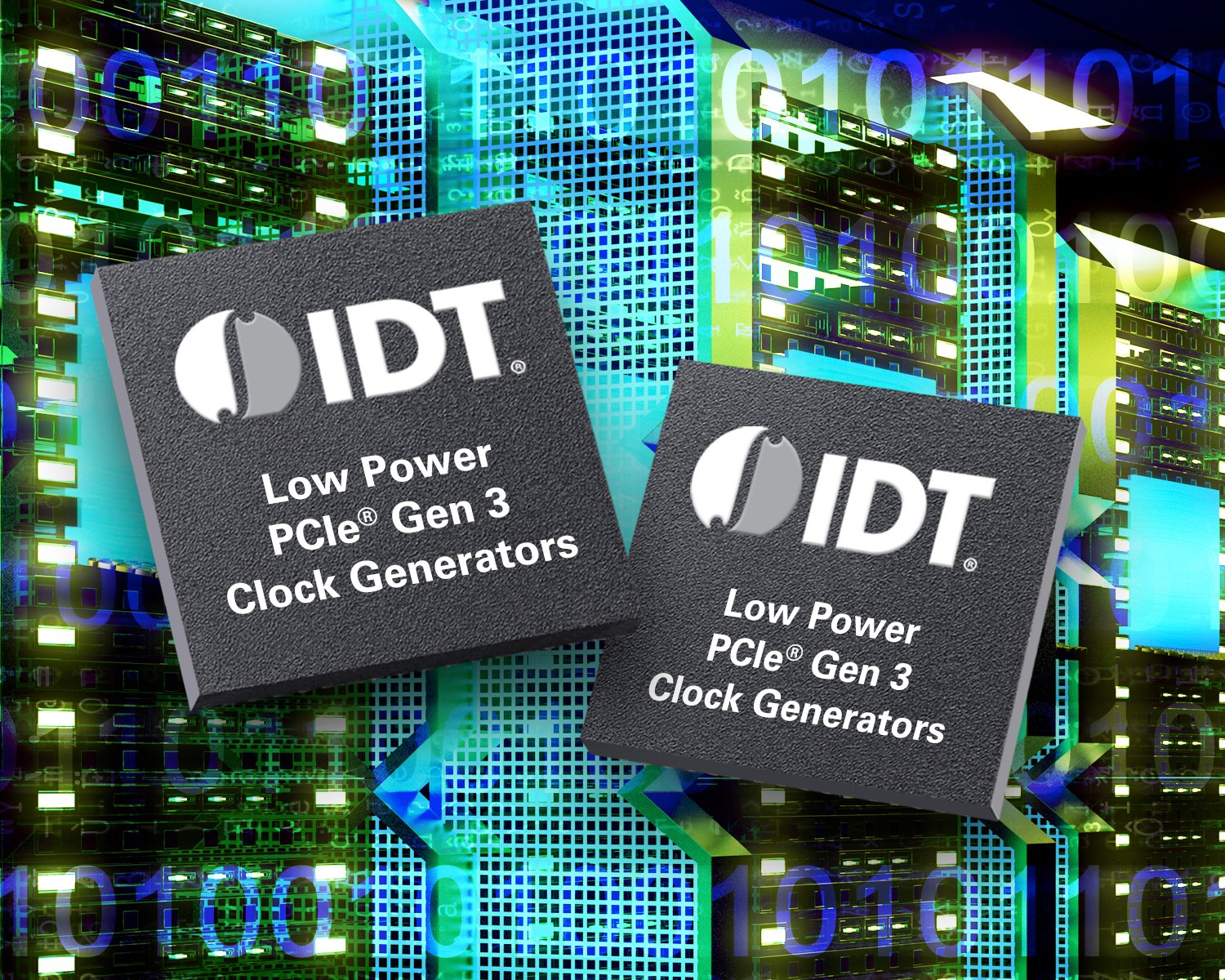
Integrated Device Technology announced the addition of 6 and 8 output 3.3 V clock generators to its low-power PCI Express (PCIe) portfolio of clock generators. The 3.3 V family of devices joins the existing 1.5 V and 1.8 V families. The new products operate at approximately 100 milliwatts, making them the lowest power 3.3 V PCIe clock generators on the market. By operating at roughly one-fifth the power of traditional PCIe clock devices, the IDT 3.3 V devices effectively eliminate thermal concerns.
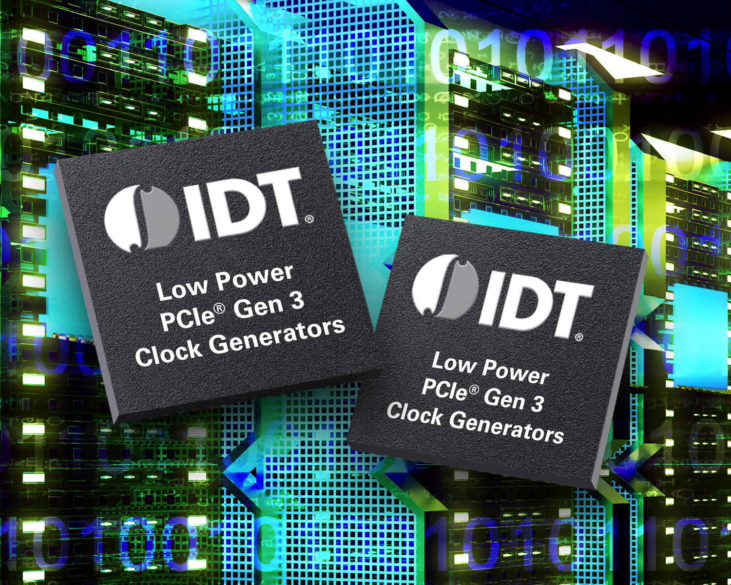
With their integrated terminations, the 9FGL06 and 9FGL08 devices’ ultra-compact 5×5- and 6×6-millimeter packages can deliver up to a 90 percent reduction in board area. Factory programmable versions provide quick turn device optimizations to meet exact customer requirements. The SoC-friendly devices greatly exceed the phase jitter requirements of the PCIe Gen3 specification in anticipation of the upcoming PCIe Gen4 specification, and are also suitable for applications needing less than 3ps rms 12k-20M phase jitter, such as gigabit Ethernet and other high-performance applications..
“With our release of the 9FGL family, IDT adds 3.3 V devices to its portfolio of low-power, high-performance PCIe clock generators delivering the features that meet our customers’ needs to reduce space and power,” said Kris Rausch, general manager of IDT’s multi-market timing division. “And looking to the future, we fully expect these new devices to meet the requirements of the coming PCIe Gen4 standards.”
The 3.3 V devices are pin-compatible to IDT’s highly successful 1.5 V 9FGU-series and 1.8 V 9FGV-series PCIe clock generators. The timing family targets power- and space-constrained designs in both consumer and high-performance applications, providing enterprise-level performance while lowering the total cost of ownership. Potential applications include multi-function printers, servers, set-top boxes and solid state drives. The entire family is compliant with PCIe generations 1, 2 and 3.
The 3.3 V (L-series) family offers industry firsts that include:
• Output-by-Output configuration of output impedances, allowing a single part to be used in mixed impedance environments without external termination components.
• Factory programmable versions that allow user-defined default configurations including output impedance, control input polarity, internal pull up or pull down resistors, and wake-on-LAN mode for the crystal oscillator. This removes the need for practically all external glue logic.
IDT plans to quickly follow this initial offering with 3.3 V versions of low-power PCIe buffers and multiplexers that are pin-compatible to the successful 9DBU/V and 9DMU/V families
The 9FGL PCIe clock generator family includes devices with 2, 4, 6, or 8 outputs. The clock generators support both the PCIe Common Clock architecture with or without spread spectrum, and the PCIe Independent Reference (IR) clock architecture (non-spreading). The devices also provide a copy of the reference clock, saving a crystal in the design.
The 6-output 9FGL06xx and 8-output 9FGL08xx PCIe clock generators are available now. The 2-output 9FGL02 and 4-output 9FGL04 clock generators will be available in Q3, 2015.


