
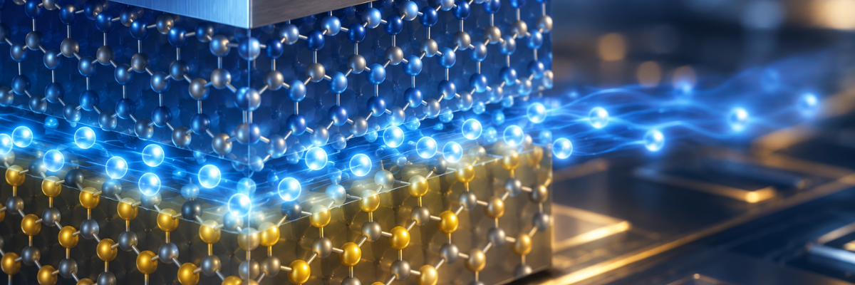
Gallium nitride (GaN) has become an important semiconductor for high-power and high-frequency electronics, in part because engineers are able to take advantage of something that happens where GaN meets another material.
At certain interfaces, differences in polarization create an extremely thin layer where electrons become concentrated. Known as a two-dimensional electron gas (2DEG), this layer provides the high-density, high-mobility channel used in devices such as GaN high-electron-mobility transistors (HEMTs).
The materials surrounding GaN therefore matter almost as much as the GaN itself. Change the material at the interface and engineers potentially gain another way to control how many electrons are available to carry current.
Researchers in Japan have now expanded those options with an unusual addition: niobium.
A team from Tokyo University of Science, the University of Tokyo and Mie University has created niobium aluminum nitride (NbAlN) as a single-crystal polar semiconductor on GaN. When the researchers incorporated the material into a GaN-based heterostructure, the electron density at the AlN/GaN interface increased by more than three times compared with a structure without NbAlN. The results were published September 3 in Advanced Materials.
Why Add Niobium?
Aluminum nitride (AlN) and GaN belong to a family of materials known as polar wurtzite nitride semiconductors. Along with properties such as wide bandgaps and high breakdown fields, their crystal structures produce strong polarization.
That polarization is useful in GaN electronics.
At an AlN/GaN interface, a difference in polarization between the two materials causes electrons to accumulate without requiring conventional intentional doping. The resulting 2DEG forms a conductive channel with high carrier density and mobility.
One way to change the characteristics of these materials is to introduce other elements. Scandium, for example, has been added to AlN to significantly alter its lattice and polarization-related properties.
Transition metals present a harder problem.
Niobium normally favors metallic bonding. Incorporating it into AlN while maintaining the wurtzite crystal structure and the consistent polarity needed for the material’s useful electronic properties is difficult.
The researchers wanted to see whether they could do both.
Using reactive sputter epitaxy, the team grew NbAlN films containing between 11 and 37 percent niobium on GaN. Films containing up to 25 percent niobium maintained a smooth surface and coherent wurtzite structure aligned with the underlying GaN. At 37 percent, however, the surface became substantially rougher and crystal quality deteriorated.
Atomic-resolution microscopy provided an even closer look. In an approximately 25-nanometer-thick film containing 23 percent niobium, the researchers found that the NbAlN maintained the same metal-polar orientation as the GaN beneath it.
Even nanoscale regions containing higher concentrations of niobium did not interrupt the continuous wurtzite lattice.
In other words, the researchers had managed to introduce a transition metal without losing the crystal structure and polarity they were trying to preserve.
More Electrons at the Interface
Creating NbAlN was only part of the experiment. The next question was whether its unusual structure would provide a useful electronic property.
The researchers added NbAlN as a barrier layer in an NbAlN/AlGaN/AlN/GaN heterostructure and measured the 2DEG at the AlN/GaN interface.
Without NbAlN, the sheet electron density was approximately 5.1 × 10¹² electrons per square centimeter.
With the NbAlN barrier, it reached 1.7 × 10¹³ electrons per square centimeter, an increase of more than three times. The researchers also reported that the structure maintained high electron mobility.
The team attributes the change to carrier modulation associated with the polarization of the NbAlN barrier.
That distinction is important. The work is not simply about squeezing more electrons into a semiconductor. It demonstrates another material engineers could eventually use to manipulate the polarization conditions that determine how carriers behave at a GaN interface.
“NbAlN belongs to a previously unrecognized class of transition-metal-containing polar nitride semiconductors,” said Atsushi Kobayashi, associate professor at Tokyo University of Science and corresponding author of the study.
Why Electron Density Matters
For a GaN HEMT, the 2DEG forms the channel between the device’s source and drain. Applying voltage to the gate controls current through that channel.
The ability to engineer its carrier density is therefore an important part of designing GaN heterostructures.
A higher 2DEG density potentially provides more charge carriers for conduction, making the result interesting for high-power and high-frequency electronics. But higher carrier density alone does not guarantee a better transistor.
Mobility matters too. So do breakdown behavior, leakage, interface quality, thermal performance, reliability and the ability to manufacture the structure consistently.
The latest study did not demonstrate a finished transistor with three times the performance of an existing GaN device. Instead, it demonstrated something more fundamental: NbAlN provides another way to change the electronic conditions inside a GaN heterostructure while retaining the polar crystal structure required to produce those effects.
That gives device designers another material variable to explore.
Expanding the GaN Material Toolbox
The work also has implications beyond this particular NbAlN/GaN structure.
The researchers demonstrated that a transition metal with strong metallic characteristics could be incorporated into a polar nitride while preserving its functional asymmetry. Until now, the difficulty of maintaining the wurtzite structure and polarity has limited the range of elements available for this type of materials engineering.
The result potentially opens a broader family of transition-metal-containing polar nitrides for investigation.
There are still limits to determine. The decline in crystal quality at higher niobium concentrations shows that adding more of the element is not necessarily better. The researchers also need to characterize NbAlN’s polarization properties more precisely and determine how the material behaves when incorporated into working electronic devices.
For GaN electronics, however, the research introduces a new design option.
The next advance in GaN does not necessarily have to come from changing GaN itself. It might come from engineering the materials around it.
Original Source: https://www.t.u-tokyo.ac.jp/en/press/pr2026-09-07-001