At the 2018 Symposia on VLSI Technology and Circuits, imec will present a process flow for a complementary FET (CFET) device for nodes beyond N3. The proposed CFET can eventually outperform FinFETs and meet the N3 requirements for power and performance. It offers a potential area scaling of both standard cells (SDC) and memory SRAM cells by 50%.
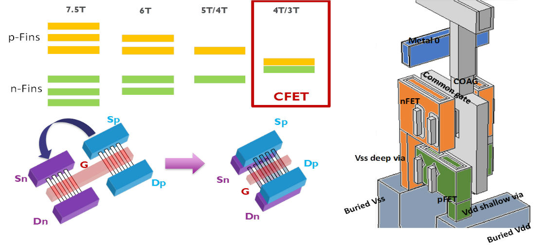
The CFET is a further evolution of the vertically stacked gate all around nanowire transistor. Instead of stacking either n-type or p-type devices, it stacks both on top of each other.
Imec’s proposed flow consists of stacking an n-type vertical sheet on a p-type fin. This choice exploits the FinFET process flow and benefits from the potential for strain engineering in the bottom pFET. Buy Cialis
Based on TCAD analysis, the proposed CFET can meet the N3 targets for power and performance, where it will outperform FinFETs.
However, the dominant parasitic resistance of the deep vias needs to be reduced. This can be achieved by introducing advanced Middle of Line (MOL) contacts using e.g. ruthenium.
50% Area Reduction
A design-technology co-optimization (DTCO) analysis reveals that the CFET device used in either an SDC or SRAM cell has the potential of 50% area reduction.
The SDC area is mostly driven by accessing the transistor terminals. Consequently, the area gain using CFETs will not lie in the reduction of the active footprint, but rather in the considerable simplification of the transistor terminal access.
By fully benefiting from the CFET architecture, it is possible to reduce the SDC to three routing tracks whereas the most advanced FinFET libraries today need six.
For SRAM cells, the same area reduction is possible thanks to a new cross-coupling scheme that allows us to scale the cell height from T6 to T4.
“Given its excellent characteristics and scaling potential, the CFET device is an excellent contender for the new device architecture we need for nodes beyond N3, pushing the horizon for Moore’s Law farther out,”
stated Julien Ryckaert, distinguished member of the technical staff at imec.”
These results will be presented on the 21st June at the VLSI Technology Symposium, in session T13: FET performance and scaling.
This research is performed in cooperation with equipment companies TEL Coventor and Lam Research and with imec’s key program partners including GlobalFoundries, Huawei, Intel, Micron, Qualcomm, Samsung, SK Hynix, Sony Semiconductor Solutions, TOSHIBA Memory, TSMC and Western Digital.