At the IEEE IEDM 2018 conference, imec, the research and innovation hub in nanoelectronics and digital technologies, presented a demonstration of 3D stacked FinFETs on 300mm wafers using a sequential integration approach with a 45nm fin pitch and 110nm poly pitch technology.
The top layer consists of junction-less devices fabricated at a temperature below 525°C in a silicon layer transferred by wafer-to-wafer bonding. The high performance of the resulting stack demonstrates how the 3D sequential approach can be deployed to obtain an aggressive device density at advanced nodes.
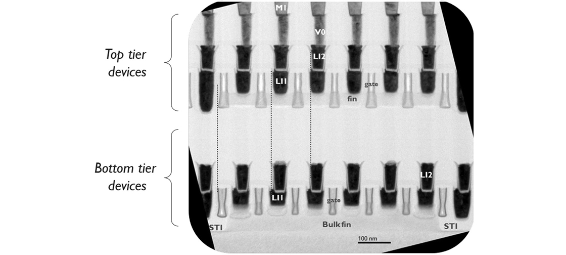
Sequential-3D integration (S3D) involves the vertical integration of sequentially processed device layers. The technique is slated to enhance device density per chip area, reduce the length of the interconnection lines, and facilitate the co-integration of heterogeneous device technologies. A major technological challenge though is the restricted thermal budget for the top layer processing.
At too high temperatures, the bottom tier devices, interconnect layers and wafer bonding dielectric may be impacted. But a limited temperature on the other hand may result in a performance degradation for the top layer and mismatch between the two tiers.
Imec first processed bottom devices using a 300mm silicon bulk FinFET flow featuring a 45nm fin pitch, a 110nm gate-pitch and a high-k last replacement metal gate. The top silicon layer is then transferred onto the bottom device layer by wafer-to-wafer bonding with a bonding dielectric stack scaled down to 160nm. On that top silicon layer, FinFET devices are then processed at a temperature below 525°C.
The high-precision alignment with the last-processed interconnects in the bottom layer is done using an immersion 193nm lithography stepper. The resulting top tier devices show a performance on par with high-temperature bulk FinFETs for low stand-by power applications (LSTP). This demonstrates the suitability of this technology to enable applications combining analog/LSTP top tier devices on High Performance (HP) bottom tier devices.
“With this process, we managed to solve many of the outstanding challenges of sequential 3D processing. An example is the extremely precise alignment of the first-processed top layer with the last-processed bottom layer, which we managed using 193nm immersion lithography,” commented Nadine Collaert, Program Director at imec. “These results demonstrate the suitability of the 3D sequential approach for an aggressive device density enhancement at future technology nodes.”