


0.3Ω dynamic resistance provides clamping voltages more than 23 percent lower than similar silicon solutions
SP1255P Series high resolution image (click here)
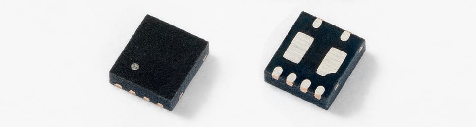
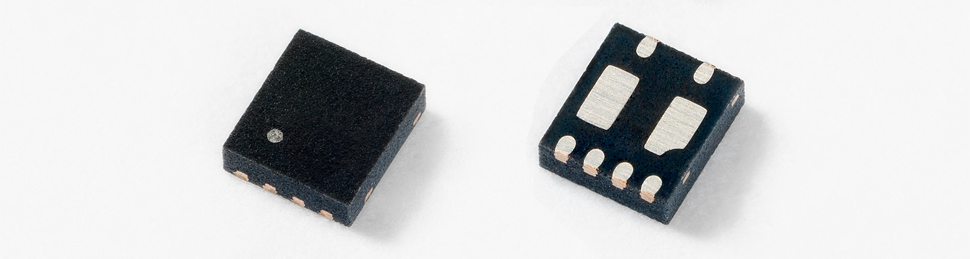
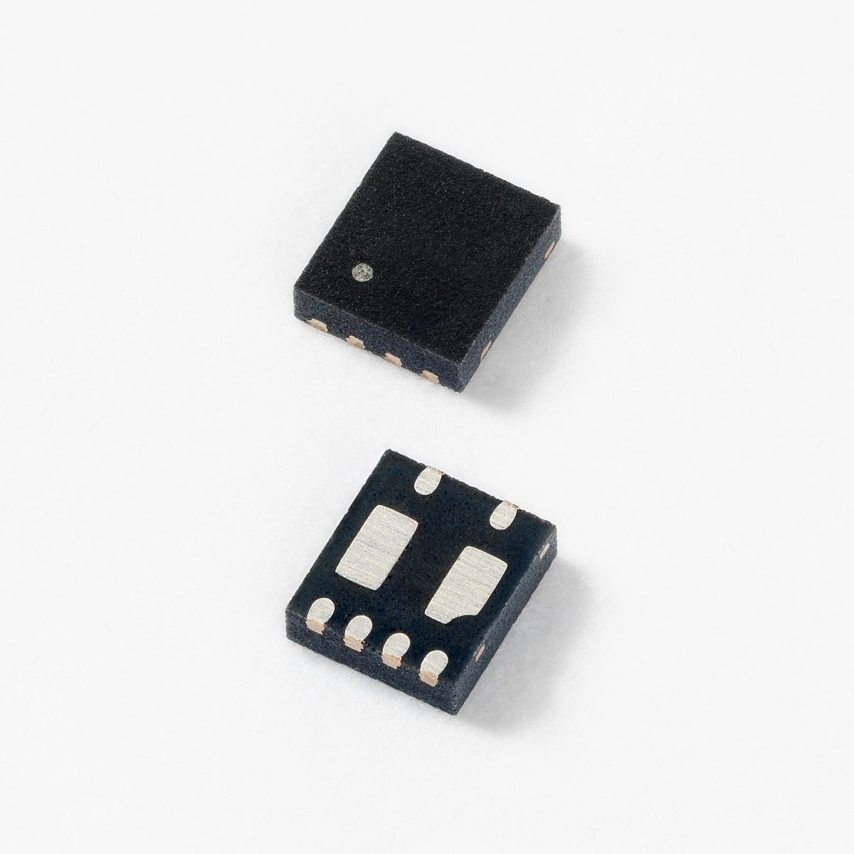
Littelfuse, Inc., the global leader in circuit protection, has introduced the SP1255P Series Low Capacitance ESD Protection TVS Diode Arrays (SPA® Diodes), which are designed to provide superior ESD protection for current-intensive applications, such as fast-charging peripherals or PoweredUSB. The SP1255P Series integrates three channels of ultra-low capacitance steering diodes with a low voltage TVS diode to provide maximum ESD protection of the USB data and ID pins per the IEC 61000-4-2 standard. With a dynamic resistance of just 0.3Ω, they provide clamping voltages up to 23 percent lower than similar silicon solutions. A high surge current protection device with a working voltage of 12V is allocated for Vbus protection; this device protects against lightning level fast transients of up to 100A on the USB Vbus line.
Typical applications for the SP1255P Series include ESD protection for smartphones, tablets, and other portable electronics.
“The SP1255P Series offers a new approach to protecting the charging functions of tablets and smartphones against high current fast transients, whether they’re induced by nature or by erratic electrical grids,” said Chad Marak, Product Line Director for the TVS Diode Array line. “Their space-saving footprint and low profile make them ideal for ESD protection applications in a variety of portable consumer electronics where board space is at a premium.”
SP1255P Series Low Capacitance ESD Protection TVS Diode Arrays offer these key benefits:
• Low dynamic resistance of 0.3Ω provides clamping voltages up to 23 percent lower than similar silicon solutions to offer superior protection for current-intensive applications such as fast-charging peripherals.
• Robust ESD capability for Vbus or USB data pin protection allows manufacturers to claim ESD protection above the maximum level as stated in the IEC standard.
• Small form factor µDFN-6 package (1.8×2.0x0.55 mm) simplifies the PCB layout by allowing the traces to run directly underneath the device without the need for stub traces that can cause signal degradation.
• Automotive-grade quality (AEC–Q101 qualified) ensures maximum reliability in the harshest environments.


