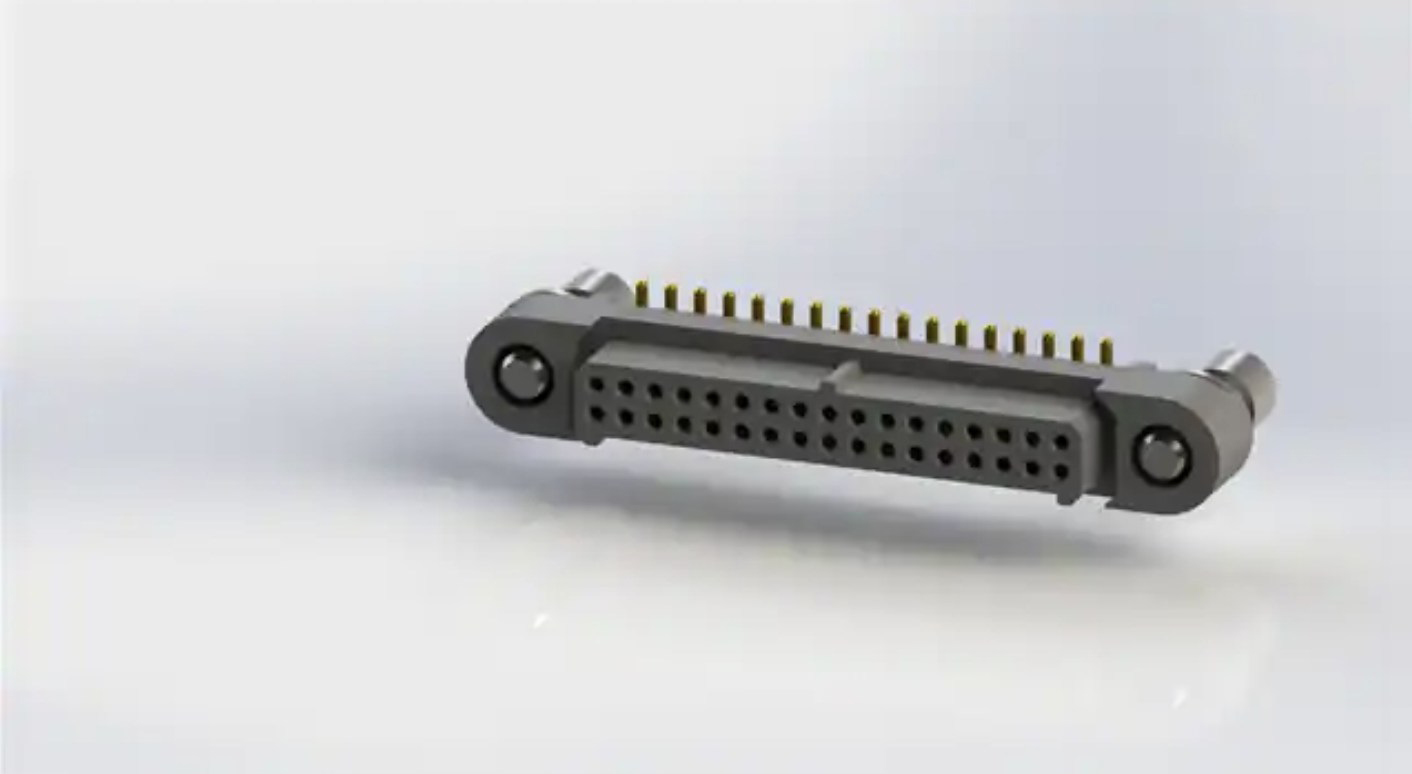
Altering Nanowire Cell Structure Allows Tuning Over Wide Energy Ranges

By Ruth Seeley

If tiny nanowire semiconductors could actually convert electricity into light and back again at the right wavelengths, their potential to speed up computers, make solar cells more efficient, and make LEDs more colorful would be achievable.

Recently a research team at the German Helmholtz-Zentrum Dresden-Rossendorf (HZDR) has managed to produce nanowires with operating wavelengths that can be freely selected over a wide range simply by altering their shell structure. This means fine-tuned nanowires could take on several roles in an optoelectronic component, making the components more powerful, more cost-effective, and easier to integrate.

Known for their versatility, nanowires can be used for miniaturized photonic and electronic components in nanotechnology. Applications include optical circuits on chips, novel sensors, LEDs, solar cells and innovative quantum technologies. Free-standing nanowires ensure the compatibility of more recent semiconductor technologies with conventional silicon-based technologies. Since contact with the silicon substrate is tiny, they surmount typical difficulties in combining different materials.

For their study, which lasted several years, the Dresden researchers first set about growing nanowires from the semiconductor material gallium arsenide on silicon substrates. The next step involved enclosing the wafer-thin wires in another layer of material to which they added indium as an additional element. Their goal: the mismatched crystal structure of the materials was intended to induce a mechanical strain in the wire core, which changes the electronic properties of gallium arsenide. For instance, the semiconductor band gap becomes smaller and the electrons become more mobile. To magnify this effect, the scientists kept adding more indium to the shell, or increased the shell’s thickness. The result went way beyond expectations.

Taking a known effect to extremes

“What we did was take a known effect to extremes,” explained Emmanouil Dimakis, leader of the study that involved researchers from HZDR, TU Dresden and DESY in Hamburg. “The 7% of strain achieved was tremendous.”

At this level of strain, Dimakis had expected to see disorders occurring in the semiconductors: in their experience, the wire core bends or defects arise. The researchers believe that the special experimental conditions were the reason for the absence of such disorders: First, they grew extremely thin gallium arsenide wires that were around five thousand times finer than a human hair. Second, the team managed to produce the wire shell at unusually low temperatures. Surface diffusion of atoms is then more or less frozen, forcing the shell to grow evenly around the core. The team of researchers reinforced their discovery by conducting several independent series of measurements at facilities in Dresden, as well as at the high-brilliance X-ray light sources PETRA III in Hamburg and Diamond in England.

The extraordinary results led the researchers to undertake further investigations: “We shifted our focus to the question of what triggers the extremely high strain in the nanowire core, and how this can be used for certain applications,” Dimakis recollected. “Scientists have been aware of gallium arsenide as a material for years, but nanowires are special. A material may exhibit completely new properties at the nanoscale.”

The researchers realized that the high strain let them shift the bandgap of the gallium arsenide semiconductor to very low energies, making it compatible even for wavelengths of fiber-optic networks.

Source: HZDR

Leave A Reply

Your email address will not be published.