


By Camille Bianca Gomez, Senior Product Applications Engineer, Analog Devices
Power management in field programmable gate arrays (FPGAs), application-specific integrated circuits (ASICs), and other multirail processor-based systems is growing increasingly complex as sequencing rules tighten, timing requirements become more precise, and voltage tolerances shrink. Incorrect sequencing can trigger latch-up or permanent device damage, while insufficient monitoring can delay fault detection and compromise system stability.
This article presents practical strategies for optimized timing coordination and fault response, demonstrating how an 8-channel sequencer with integrated supervision and factory-trimmed settings simplifies power management compared with basic supply-sequencer solutions.
Introduction
Field programmable gate arrays (FPGAs) are increasingly used in artificial intelligence (AI), data centers, healthcare, and industrial automation to deliver high-throughput, low-latency computation. Their combination of hardware configurability and highly parallel processing makes them well suited for real-time workloads with large data volumes.
Power design for FPGAs is rarely a single-rail problem. These devices use multiple supply domains: core, input/output (I/O) banks, phase-locked loops (PLLs), high-speed transceivers, and auxiliary rails, and each domain has its own voltage level, current profile, and margin requirements. A solid power delivery network must do more than generate the rails; it must bring them up and down in a controlled way and keep them inside their allowable windows during transients and fault conditions.
In practice, FPGA power requirements usually boil down to these design checks:(1,2)
- Multiple Rails: Provide dedicated supplies for core, I/O, PLL, transceivers, and auxiliary domains.
- Low-Voltage Core Accuracy: The core rail often runs at the lowest voltage to reduce power, so regulation accuracy and load-step response matter.
- Tight Rail Tolerance: Each rail has its own allowed voltage window (margin) for stable
- Controlled Ramp-Up: Manage ramp rate and inrush so internal circuits start cleanly and rails don’t collapse or overshoot.
- Power Sequencing: Follow the required rail order at turn-on and turn-off, including reverse sequencing constraints.
Voltage regulators handle generation and regulation, but they don’t always guarantee timing, sequencing, and continuous window monitoring across all rails, especially during brownouts, faults, or power-down events. That’s why FPGA power management designs necessitate external sequencers and voltage supervisors to coordinate rail timing and monitor thresholds throughout operation.
Controlling Thresholds and Timings: Supervisors + Sequencers in Practice
Sequencers and voltage supervisors explicitly implement timing and voltage thresholds for each rail. A multichannel sequencer can hold off the next rail until the current rail is within a defined window of its target voltage, then apply a controlled delay before enabling the next rail. This helps ensure monotonic, glitch-free ramping.
High-quality supervisors offer multivoltage monitoring with threshold accuracy as tight as ±0.3% while supporting power-on reset, proper sequencing, and continuous monitoring by asserting reset signals whenever any rail falls outside the specified range. (3,4) In practice, supervisors can trigger a controlled FPGA reset or safe shutdown during undervoltage or overvoltage to prevent erratic behavior. When combined with a sequencer, they ensure the correct startup order and provide continuous system health supervision across all rails.
Analog Devices offers a broad portfolio of power-sequencing integrated circuits (ICs) with supervision, including the MAX16050, MAX16165, and MAX16025. The newest addition is the ADM6840, a configurable sequencer with integrated supervision that supports up to eight power rails, purpose-built for advanced FPGA and system on a chip (SoC) platforms. By managing all eight rails in one device, it reduces external components and complexity compared with typical 4-channel solutions.
Optimized Monitoring and Sequencing Architecture for a Simplified Solution
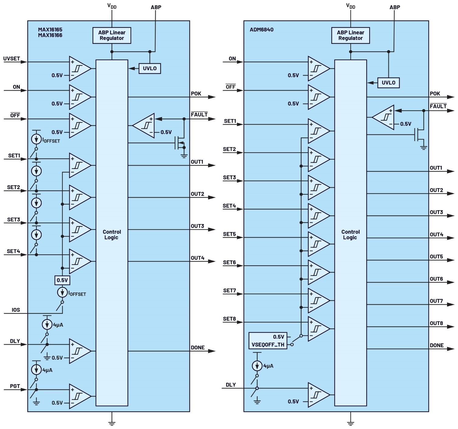
The ADM6840 retains the core sequencing and supervision functionality of established ADI supply sequencers such as the MAX16165/MAX16166, while extending support to up to eight power rails in a simpler, more optimized implementation as shown in Figure 1. This is achieved by converting key externally configured functions into factory-trimmed internal options, which improves accuracy, consistency, and repeatability across builds and reduces sensitivity to component tolerances and printed circuit board (PCB) leakage. These factory-trimmed options include offset current setting (IOS), which shifts the falling threshold for reliable reverse-order turn-off; power-good timer (PGT), which limits how long a rail may take to reach its SET monitored threshold during sequencing; and an undervoltage sensing input (UVSET), which provides a typical 0.5V threshold input to monitor VDD or another supply.
Daisy-Chaining Multiple Sequencers for More Complex Power Trees
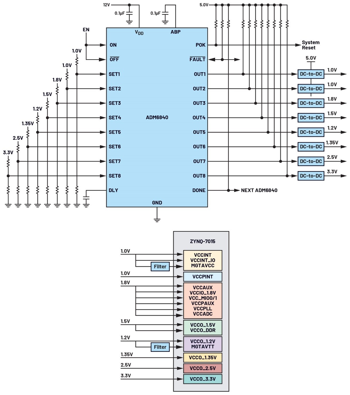
The high-channel density of the ADM6840 allows a single device to support eight power rails on an FPGA as illustrated in Figure 2, eliminating the need to cascade two power sequencers and reducing component count and inter-device dependencies.
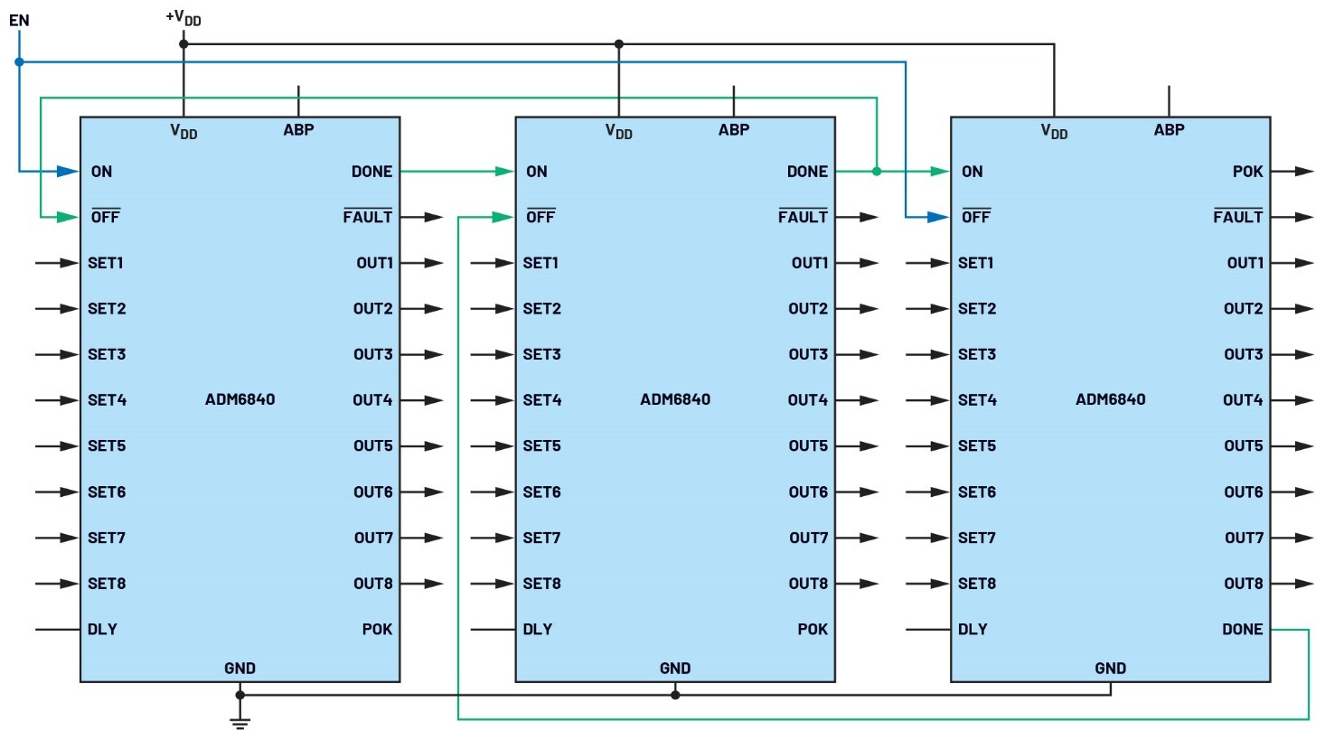
While it supports up to eight power rails in a single device, it is also fully capable of daisy-chaining multiple ICs to accommodate even larger or more complex FPGA power trees such as the configuration shown in Figure 3. Designers can link devices using the DONE, ON, and OFF pins, maintaining coordinated sequencing across all rails. This flexibility allows system architects to scale beyond eight channels if required, while still benefiting from this simplified design.
Power-Good Timer and Power-Down Sequencing for Precise Timing Requirements
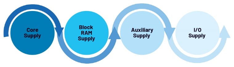
During power-up sequence, timing requirements are important: a given voltage rail must ramp up toward its nominal value within a defined window before the next rail is allowed to begin powering up. For modern FPGAs and adaptive SoCs, the rails must ramp monotonically and reach their final voltages within a specified ramp time. For example, in XAPP1375, the voltage must reach ≥95% of its final value within a defined ramp period before the next rail in the sequence begins to ramp up.5 This approach helps ensure that the device exits the power-on reset (POR) state correctly and avoids issues caused by slow or improper rail rise behavior. FPGA vendors such as AMD or Altera provide a recommended power-up sequence in their data sheets and may vary between FPGA families. An example of power-up sequencing implementation is shown in Figure 4.
The power-good timer verifies that each supply reaches its set threshold voltage within a defined window during the power up sequence. In the ADM6840, this delay is factory-trimmed, offering multiple options rather than being set by an external capacitor, which ensures consistency and repeatable timing. With an external capacitor, the delay accuracy can be affected by the capacitor’s leakage and tolerance, potentially leading to variations in timing.
Additionally, power-down sequencing requires careful control of stored energy to ensure predictable shutdown timing and to prevent damage to devices. High-power rails often include large bulk electrolytic capacitors that stay charged during shutdown and can release enough energy to harm components that aren’t properly protected. With this, FPGA vendors like Altera provide their recommended power-down sequencing to mitigate the risk.6 In general, the recommended power-down sequencing is the reverse order of the power-up sequence.
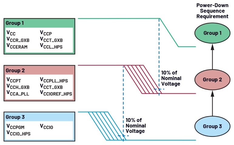
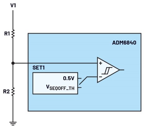
For example, in the Altera Arria 10 device, during power-down sequencing, each group of rails must drop to less than 10% of its nominal voltage before the next group begins to power down, as illustrated in Figure 5.6 To address this type of requirement, the ADM6840 implements factory-trimmed power-down threshold (VSEQOFF_TH) options 0.333V, 0.167V, and 0.050V. In comparison to other sequencers, the power-down threshold can be set through external component programming, such as with resistors or capacitors, which can introduce variation in the actual power-down threshold due to resistor tolerance and PCB leakage. Figure 6 shows the simplified diagram of factory-trimmed power-down threshold implementation.
Conclusion
Meeting strict FPGA power-delivery requirements is difficult, especially with multiple supply rails, tight tolerances, and sequencing constraints. The ADM6840 simplifies this challenge by combining eight channels of sequencing and supervision in one device, while still supporting daisy-chaining to scale to larger power trees without added complexity. Factory-trimmed settings help implement recommended power-up and power-down sequences with consistent, repeatable timing—avoiding variations that can come with external components and board-level leakage. Beyond sequencing, integrated supervision enables faster fault detection and a defined response when a rail drifts outside its allowed window, supporting controlled reset or safe shutdown behavior to protect the FPGA and surrounding circuitry. As a result, the device provides a practical and reliable approach to multirail FPGA power management, helping designers achieve predictable, safe, and efficient system behavior.
References
1“Voltage Regulator Selection for FPGAs.” Altera, November 2008.
2“FPGA Power Sequencing Requirements.” Altium, July 2025.
3“Supervisory and Sequencing Devices for AMD and Intel FPGAs.” Analog Devices, Inc., 2024.
4Greg Sutterlin. “Supervisors in Multivoltage Systems.” Maxim Integrated, November 2003.
5“Simplified Power Sequencing (XAPP1375).” AMD, May 2025.
6Nathan Enger. “Care and Feeding of FPGA Power Supplies: A How and Why Guide to Success.” Analog Dialogue, November 2018.
About the Author
Camille Bianca Gomez is a product applications engineer at Analog Devices, handling protection controller products. She joined the company in March 2022, initially focusing on support and product development for high-performance supervisory products before transitioning to her current role. She obtained her bachelor’s degree in electronics engineering from De La Salle University—Laguna Campus. Prior to Analog Devices, she worked for 3.5 years as a design engineer in the automotive manufacturing industry, gaining valuable experience in engineering design and product development.